

Successful design of broadband EMC filters necessitates consideration of the actual (broadband) response of all the components used. The correct method can vary widely for different components. The actual terminations of the filter can, under certain circumstances, nullify its effect and hence must definitely be considered.
A very convenient method of describing ferrite components is the use of measured dual-gate S parameters. This approach is above all convenient for two reasons:
1. There is no need to develop a suitable equivalent circuit.
2. The equivalent circuit is excluded as a source of error.
The use of measured S parameters is a very robust approach for describing chokes and coils. As the relevant impedances of these components is usually of the same order of magnitude or significantly higher than the reference impedance of the measuring instruments used (typ. 50 Ω), the correct measurement of the S parameters is not particularly difficult; parasitic components of the measurement set-up used do not play an essential role for the subsequent application.
In summary: The S parameter data normally provided by the manufacturers of chokes or coils can be incorporated into the simulation without any problems. Besides chokes, capacitors are also used in EMC filters. It is now common knowledge that capacitors do not behave as pure capacitances, but rather the interaction of capacitance, parasitic inductance and resistive losses shows a response comparable with a series resonant circuit (RLC). Here it is of importance to assign the correct values (L, R) for the parasitic elements.
In order to avoid agonizing over parasitic elements and as a means of elegantly circumventing a potential source of error and in the light of the aforementioned argumentation, it would appear quite logical to also use the measured S parameters for describing capacitors. But, as so often, the devil is in the details. Especially in today’s very commonplace SMD capacitors, the effective parasitic inductance is partly dependent on the capacitor used and partly from the layout geometry and the layer construction. In many cases the latter part dominates.
This is quite logical from a physical perspective: The total inductance is firstly the property of a closed circuit and can only be correctly specified, i.e. from one contact of the capacitor to the other, for example, if the complete circuit is known. But, as the circuit is only realized in the development of the specific application, precisely this condition is not fulfilled.
In other words, this means that the use of measured capacitor S parameters only promises a correct prognosis of the later filter attenuation if a comparable layout geometry is used as that in the measurement of the S parameters. However, this is generally not known and/or is not achievable in the respective application, which makes this a less attractive approach.
So, in the interests of precise simulation over a large bandwidth, both the capacitor as well as the layout geometry have to be considered and included in the calculations, e.g. in the form of suitable equivalent circuits. This task is already well known from another application area: The correct description of the capacitors used for reliable simulation of the interactions of planes and components is essential in the development of high performance and EMC optimized power systems (power planes).
Software tools developed for interpreting these power systems present themselves to a certain extent for developing broadband EMC filters, as the technology for precise simulation of the “parallel branch” already exists. Furthermore, in the context of power systems of this type, there is a specific application for such filters: Decoupling the power system from its surroundings.
For example, the 5 V voltage could come onto the circuit board via a pin out of the backplane and broadband attenuation should be introduced at just this point to prevent external interference reaching the board or to keep interference generated on the board away from the backplane (or cables).
In this special case, the parallel branch of the filter consists of the ready decoupled 5 V power system, the series branch of an optimally selected ferrite choke (Figure 1.81).
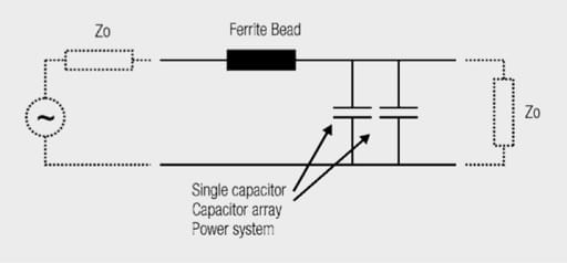

Fig. 1.81: Basic filter structure
A filter of this type is developed with the SILENT V4 software below. Here the aim is to select a chip bead from the integrated database, which most effectively supplements the properties of the parallel branch.
It should first be assumed that the properties of the PCB system are insignificant, and the impedance is only determined from the capacitors. This assumption is generally incorrect in the case of a power system. If the filter only consists of one or more parallel capacitors and a choke, this assumption agrees with reality, however. The special features of power systems will be examined in detail later on.
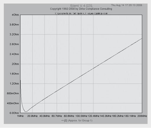

Fig. 1.82: Magnitude of impedance of a 100 nF capacitor
Figure 1.82 shows the magnitude of the impedance |Z| for an 100 nF SMD capacitor. It is immediately apparent that the capacitor has low impedance in the lower frequency range. Even if the low impedance bandwidth is expanded through parallel switching of several of the same or several correctly graduated capacitors, this situation does not fundamentally change. It may therefore make sense to select the chokes for connection in series such that they provide considerable attenuation, especially in the higher frequency range.
This results in a well balanced attenuation over a broad frequency range. Chokes with very high maximum attenuation values are generally more or less narrow band and therefore only tend to be of limited suitability for use in broadband filters. Through specific selection of a choke optimally matched to the capacitive impedance, this restriction can sometimes be overcome.
As an example, a filter is now developed which consists of three parallel 100 nF capacitors. As it is slightly inconvenient to compensate the impedance profile of these capacitors against the impedance curve of a whole range of chokes, SILENT includes a feature for filter synthesis. SILENT automatically selects those chokes from a choke database with which the required filter specification can be achieved (Figure 1.83).
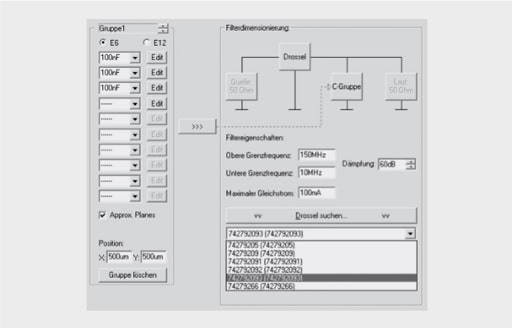

Fig. 1.83: Filter specification and choke selection
In this case a minimum attenuation of –60 dB was specified over a frequency range of 10 MHz to 150 MHz.


Fig. 1.84: Simulated insertion loss of the filter
As seen in Figure 1.84, the filter fulfils the attenuation requirement. In order to test the reliability of the simulation, the filter was constructed and measured with a network analyzer (HP8753C).
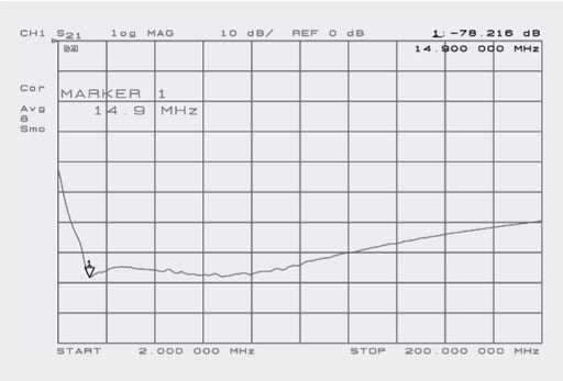

Fig. 1.85: Measured insertion loss of the filter (2–200 MHz)
The measurement (Figure 1.85) shows good agreement with the simulation; existing deviations are attributable to factors including the manufacturing and component tolerances, as well as to the inadequately specified losses in the capacitors.

Fig. 1.86: Measured attenuation of the ferrite bead
The insertion loss of the selected choke itself is shown in Figure 1.86: The choke appears to be well selected, as it shows pronounced attenuation in the upper frequency range (> ~40 MHz); in the lower frequency range – i.e. where the capacitors are of very low impedance – its attenuation drops quite quickly. Bandwidths of 500 MHz and more can be achieved with this technique without any difficulties.
At very high frequencies, the capacitors in the parallel are of high impedance sooner or later and the filter attenuation drops significantly. The exception here is filtering of power systems as previously mentioned. If the parallel capacitor array of the filter is an optimally configured power system, it can be of very low impedance even into the GHz range. If this parallel capacitor array is now supplemented with a suitable choke, considerable attenuation can be achieved up to 2 GHz and beyond.
The use of this filter is a very effective measure for reducing differential mode radiation from power systems, as this radiation typically shows a very pronounced broadband interference level due to the large number of active digital components.But let us return to our “classical” filter, consisting of three 100 nF capacitors parallel and a choke (742 792 093) in series and its insertion loss shown in Figure 1.84 and Figure 1.85. In simplified terms, the insertion loss specifies how much less power is converted in the load as a result of the filter inserted.
Insertion loss


Looking at the formula for calculating insertion loss (Equation 1.79), it is immediately apparent that besides the impedance of the filter, also the source and load impedance affect the result (POUT = UOUT2/ZOUT). For measuring instruments (e.g. network analyzers), the convention has become established as the industry standard of using both the source and load impedance as R = 50 Ω. Logically, this convention is also applied for the simulation of filters. The source and load impedances that EMC filters encounter in their subsequent applications are generally dissimilar and are also nothing like 50 Ω, but some other (complex) impedance instead.
This, however, means that it is only possible to predict the insertion loss of a filter if the actual terminations ZIN(f) and ZOUT(f) are known. For manufacturers of EMC filters for example, this condition can practically never be fulfilled, as the manufacturer cannot know at all in which environment the customer will later use their filter.
It is therefore quite common to specify filter attenuation curves for ZIN = ZOUT = 50 Ω, and at least to allow a certain comparability between filters. Unfortunately the nagging doubt remains of not really knowing what kind of attenuation profile the filter will actually produce. In order to give an impression of what has to be expected in the worst possible case, the so-called “approximate worst case method” was defined in CISPR 17.
This involves considering the filter in two different termination combinations:
1. ZIN = 0.1 Ω, ZOUT = 100 Ω
2. ZIN = 100 Ω, ZOUT = 0,1 Ω
For filters which, for example, only consist of a single series choke, both cases result in the same attenuation profile – the filter is symmetric. As significantly higher attenuation can be achieved by using a parallel impedance (e.g. capacitor), an L structure – as with the SILENT filters – is very common. Nevertheless, there is a dramatic difference between the two CISPR-17 attenuation profiles for this type of filters (Figure 1.87).


Fig. 1.87: Insertion loss of the filter for various terminations
Whereas the 0.1/100 curve even promises slightly higher attenuation, the attenuation of the 100/0.1 combination is around 50 dB (!) poorer than the 50 Ω profile. Looking at the filter circuit in Figure 1.81, this is easy to explain: The filter termination (load impedance) of 0.1 Ω is connected in parallel with the capacitors. If the impedance of the capacitors at the observed frequency is greater than the 0.1 Ω of the load, the larger proportion of current flows through the load where it converts POUT accordingly (cf. Equation 1.79). At the other extreme, i.e. with a load impedance of 100 Ω, the capacitors are of comparatively very low impedance so the majority of the interference current flows through the capacitors and not through the load.
This relationship can be clearly shown: The choke on its own provides attenuation of around –20 dB at 40 MHz and 190 MHz (Figure 1.86). Taking a look now at Figure 1.87, the attenuation difference between the 50 Ω curve (– – – curve) and the 100/0.1 case (red curve), it is apparent that this “mismatching“ at 40 MHz leads to a decline in attenuation of around 48 dB, however only around 36 dB at 190 MHz. As the choke shows the same attenuation at both frequencies, the difference of approx. 12 dB is attributable to the parallel branch.
This is very much lower impedance at low frequencies (40 MHz) than at higher frequencies (190 MHz) and therefore makes a greater contribution to the overall attenuation at lower frequencies. If the parallel branch is now rendered largely ineffective by the 0.1 Ω termination connected in parallel, the damage at low frequencies is especially high.
This insight allows several specific recommendations for action to be derived:
• The attenuation profile from the datasheet should therefore be takenas a first information only!
• If the L filter structure described above is used, take care that the capacitor is on the side of the filter where the higher terminal impedance is expected!
• The “safe bet”: If you don’t wish to think about the terminal impedances at all or measurement/estimation is not possible, the filter is expanded to a T structure using a further choke of the same type . This increases the attenuation once again, but, above all, the filter is tolerant towards low impedance terminations . This approach saves development workload at the expense of higher unit costs and is therefore not recommended for larger series.
For the sake of completeness, it should be mentioned that, particularly for larger unit volumes, it can be extremely useful to determine the terminations in the actual component group by measurement or simulation in order to then develop both a performance and cost optimized filter with the aid of suitable simulation software.
ABC of CLR: Chapter L Inductors
Design of optimized EMC filters for real operating environments
EPCI licensed content by: Würth Elektronik eiSos, Trilogy of Magnetics, handbook printouts can be ordered here.
![]()
This page content is licensed under a Creative Commons Attribution-Share Alike 4.0 International License.
