

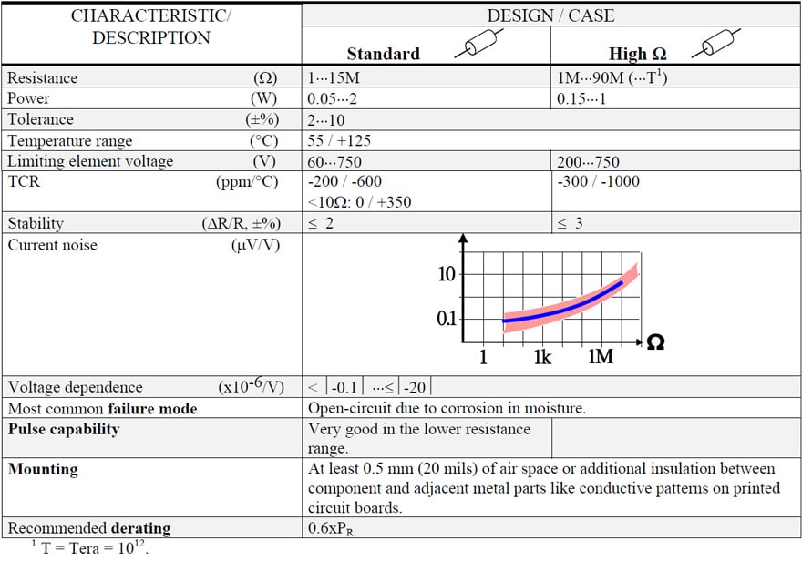
R 3.7 CARBON FILM
Carbon film resistors sometimes are called surface layer resistors. Better qualities are classified as “stable” with a ΔR/R that will stop at ≤1%. Their role has, to a great extent, been taken over by the metal film but they still have a market, especially as cheap 5 per cent E 24 components. At new designs one should yet consider replacing them with metal film resistors that also are offered in E 24, 5 per cent.
If we apply crystalline carbon on ceramic rods in a vacuum chamber or if we heat them up to temperatures close to 1000 °C and then let them be hit by hydrocarbons, carbon will be deposited at a cracking process which will produce a stable, resistive carbon film with TCR values between –250 and –1000 ppm/°C depending on the resistance value. The thickness typically varies between 0.04 and 40 μm (1.6 and 1600 microinches). Low resistance values and corresponding thick films give an excellent pulse capability that may be further amplified if the film is non-spiraled.
Somewhere below 10Ω the manufacturers pass from carbon film to metal films (nickel, chromium-nickel or nickel-phosphorous) that is applied in a chemical bath or burning process or in an electrolytic bath. Thus, the user should carefully note in the catalogue sheets at which resistance value the TCR alters from, for example, –250 to maybe ±200 ppm/ °C.
The stability of carbon film resistors is good. The noise is comparatively high and increases with the resistance; low values may be relatively noise free, equivalent to that of the metal oxide.
High ohmic types exist in their most exclusive form in a hermetically sealed state, usually glass tubes, and may reach TΩ values (x 1012). Don’t touch such components with your fingers. Perspiring hands might be enough for shunting down the rated resistance markedly.
Table R3-4 CARBON FILM RESISTORS

R 3.8 CARBON COMPOSITION
This component type is on the point of disappearing from the market. The manufacture of certain designs has ceased. In the most cases carbon composition resistors can be replaced by other both cheaper and qualitatively better components. Nevertheless, since they are part of many older designs we therefore will discuss them.
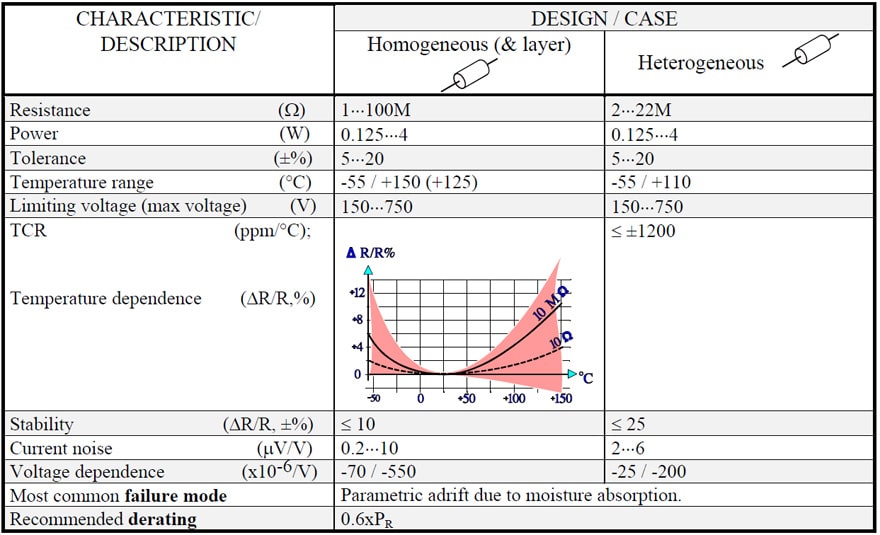
Carbon composition resistors exist in several designs: homogeneous and heterogeneous. In the first case a compound consisting of carbon powder and binder together with a resin is molded to a resistive body. In the latter case the carbon powder is mixed with a filling, usually silica or aluminum oxide, before it is molded. This type has the poorest stability and parameter characteristics. In a third variant a dispersion of graphite and binder is applied on a glass tube and then dried. The parameter characteristics of that layer type are comparable with those of the homogeneous composition type but the construction is very vulnerable.
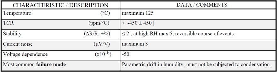
The homogeneous, molded type is qualitatively the best but also the most expensive. It is usually used in such applications where an open circuit failure mode would result in a serious safety risk. In Figure R3-8 a cutaway view is shown of homogeneous composition resistor.
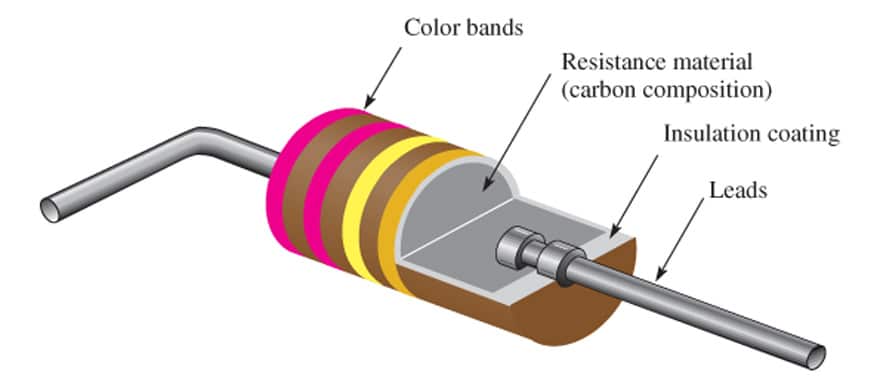

Figure R3-8. Cutaway view of homogeneous carbon composition resistor
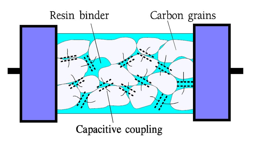

Figure R3-9. Principle sketch of the resistance element in an homogeneous carbon composition resistor.
Just as in metal glaze resistors the conduction mechanism consists of conductive granules embedded in an isolator compound (Figure R3-9). There is shown the capacitive connection between the separate carbon granules. This will lead to a strong capacitive shunting effect at higher frequencies. Some curves are shown in Figure R3-10.
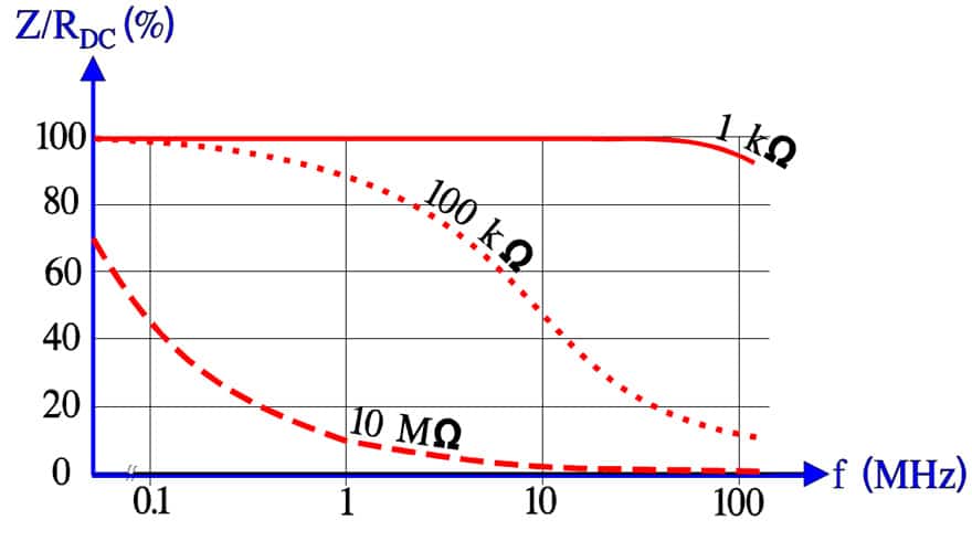

Figure R3-10. Impedance versus frequency in a ½W carbon composition resistor.
If the capacitive frequency dependence is great the inductance is the smaller. The current passes through an infinite number of branches connected in parallel which altogether creates a negligible inductance inside the resistor body. This, however, doesn’t mean that we have found the ideal component for pulse loads even if we occasionally may see such assertions. Only low resistance values, where the resistor body consists mainly of pure carbon, may correspond to such assertions. Otherwise strong surge currents might damage the uncountable contact spots in the current paths. The pulse power Pp should be limited to
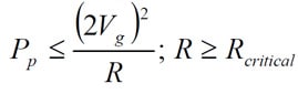

….. [R3-1]
and
![]()

…..[R3-2]
Caution! Parts from less serious manufactures may have a fire risk at improper overload conditions.
The temperature dependence is strongly non-linear. Table R3-5.
Current noise and stability are poor. The method to adjust low or decreasing resistance values by baking gives only temporary results. After some time the value is too low again. As said before, there are few reasons for choosing a carbon composition resistor.
Table R3-5. CARBON COMPOSITION RESISTORS

R 3.9 CONDUCTIVE PLASTIC
Of the fundamentally important resistance materials only one remains to be mentioned: the conductive plastic. It is closely related to the carbon composition. Actually it belongs to the potentiometer section but for consistency reasons is presented now.
If carbon powder and thermosetting plastic together with a binder are mixed together and molded we get a so called conductive plastic. It is used above all in servo potentiometers due to its low friction and excellent wear resistance. The resistance stability is fairly good provided it is not subjected to too high relative humidity or condensation.
Table R3-6. CONDUCTIVE PLASTIC RESISTORS

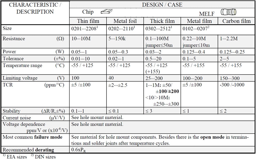
R 3.10 SMD: CHIP AND MELF
Surface Mount (SM) resistors allow a very large miniaturization. This in its turn means short conduction paths and good high frequency characteristics (Figure R1-18). Furthermore there are particular high frequency (HF) chips in thin film technique.
Fixed SM resistors are manufactured in two basic designs: as rectangular chip and as cylindrical leadless, so called MELF (Metal Electrode Face Bonding).
R 3.10.1 SMD Chip
The predominant part of all chips are manufactured with thick film, but thin film chips are becoming more and more common. Also metal foil exists as SMD. The construction is like the one in Figure R3-11. Certain types have an organic protection in one or two layers on top of the glass passivation.
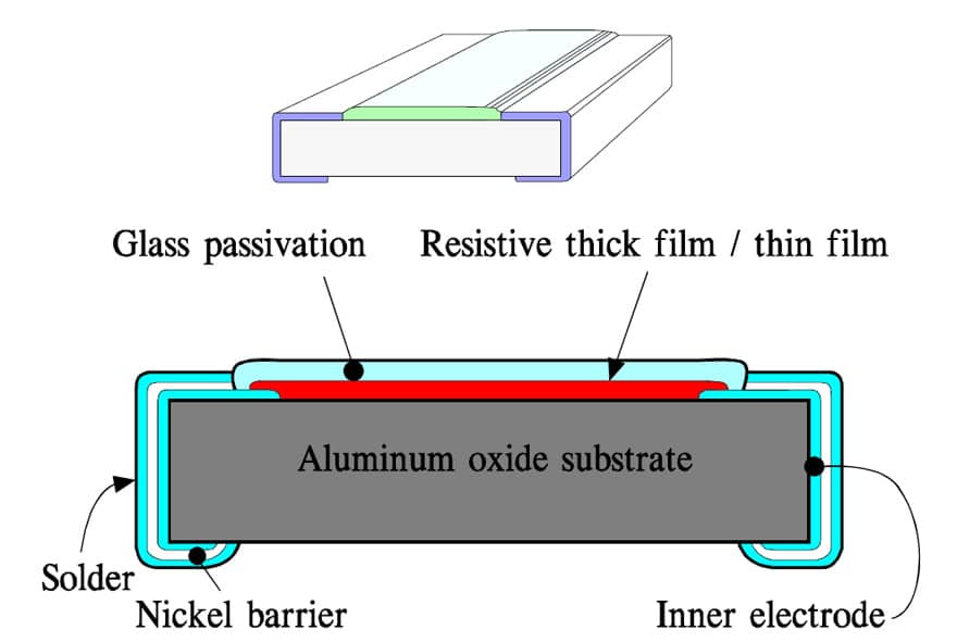

Figure R3-11. Schematic sketch of resistor chip.
The substrates are screen printed either with a metal powder paste that is fired to a metal glaze / thick film. Or metal foils are glued on a substrate or metal films are vaporized or ion implanted on it. The thick film is laser trimmed to the right resistance value by cutting a track in the long side of the film. Recent manufacturing improvements however begin making this laser trimming unnecessary. This approach without any trimming tracks will increase the pulse load capability by 2 to 3 times. The other films are designed to an inductance-reducing serpentine pattern according to Figure R3-12.
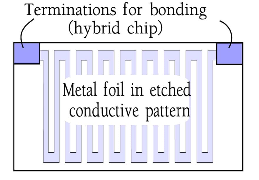

Figure R3-12. Schematic sketch of a serpentine pattern in metal foil or thin film chips.
The metal foil pattern is etched chemically or patterned by means of an ion beam. The thin metal films are applied through a mask to the desired shape.
Linear PTC designs in metal glaze are marketed. Typical data are, for example, 10 kΩ and TCR +1500 ppm/°C. Metal film chips with resistance track in a serpentine pattern also exist. Typical EIA sizes are 0603, 0805 and 1206. Common TCRs range from +150 to +4500 ppm/°C while the corresponding maximum resistance values drop from 50 kΩ to 500 Ω. The higher TCR the lower the maximum resistance which depends on the film alloys that more and more are approaching the pure metal and its correspondingly lower resistivity.
Metal foil chips exist in two designs, partly as the wrap-around according to Figure R3-11, partly for use in integrated electronics (Figure R3-12). In the latter case they are made with a protective glass passivation and with bonding pads which implies separate encapsulation.
A variant of bulk metal chips are used as current sensor. The resistance element consists of a metal plate that by laser cutting can be trimmed to tolerances of ±1% at resistance values in the range of 5 to 50 mΩ. The design and its tolerances require large chip dimensions (for example 0.4×0.2”).
Sometimes metal foil chips are delivered for special custom trimming by a scribed line.
Power chip resistors exist in thick film design. Common power ratings are 1 or 2 watts. The resistance range may cover 10 mΩ … 22 MΩ with tolerances between 1 and 10 %. The heat generation requires dimensions in the magnitude of 12 x 8 or 8 x 5 mm. The terminations usually consist of tinned compliant copper plates.
Sizes
With thick film chips the main focus has been moved from the EIA size 0805 (2 x 1.25 mm) to sizes 0603 (1.6 x 0.8) and 0402 (0.8 x 0.5). Discrete thick film chips are marketed down to 0302 or 0201 (0.8 x 0.5 respectively 0.6 x 0.3 mm). The most common chip size in thin film technology is 20 x 20 mil (0.5 x 0.5 mm; EIA code 0202) but are also found conventional EIA sizes from 0201 to 2010.
Price comparison thick film – thin film
True price comparisons are difficult because of the difference between the characteristics tolerances and TCRs that are situated in different ranges. In general, thick film are cheaper to make but consume more of the material.
R 3.10.2 MELF
This component consists of a conventional resistor for hole mount, but in a form without leads. Instead one solders direct on the press-fitted naked end caps. At wave soldering the component body should be positioned with a glue lump (epoxy) to the substrate / printed circuit board.
Because the MELF design is a modified version of well-tried, well-established hole mount types, it in this SM component assimilates all the good characteristics that characterize the respective basic hole mount type. For metal film MELF this means among other things a wide resistance range, low noise characteristics, fine tolerances and TCR values and good stability. With an extra thick metal film one has in some cases improved heat dissipation and also pulse capability. High frequency capability is achieved by a so called pulsed trim cut where the spiraled conductive pattern is broken in parts, thus reducing the inductive action from the helical trim cut and thus increasing the frequency range to several GHz.
MELF components are made in metal film, carbon film and metal glaze types. Usually they are supplied with end caps of conventional components but some manufacturers use metallized terminations.
Sizes
The MELF components were introduced as leadless metal film resistors in the DIN size 0207. Today 0402 (1.5 x 3.6 mm) is the most common, not least because of its smaller risk of open mode failure in the solder joints after frequent temperature changes. However, the size 0201 (1.1 x 2.2 mm) is already well established in the consumer market.
Price comparisons
Hole mount : MELF ≈ 2 : 3.
R 3.10.3 Cross over chips / “Jumpers”
Sometimes it’s necessary to complete existing application of printed circuits by separate short-circuiting between two points. Particular components are used, so called cross overs, cross conductors or jumpers, with the lowest possible resistance. They exist both as rectangular thick film chips as well as metal film MELFs. Max resistance for the thick film chips usually is ≤50 mΩ at sizes between 0603 and 2010. Thin film MELFs in typical sizes of L x D ≈ 2 x 1.4 to 6 x 2.4 mm are specified for ≤10 mΩ.
As well as maximum resistance a maximum current is also specified for these components.
R 3.10.4 Mounting / Soldering / Gluing
It is important to remember that SM components, more than others, are influenced by temperature changes, especially for the larger component. Thus, dimensions and mounting directions are most important. See section M of ABC of CLR for SMD mounting guidelines: “Further, short and wide bodies are preferable to long and thin ones, partly for strength reasons, partly because of the inductance and with that the frequency dependence will decrease”. Still another reason is that differences in the coefficient of expansion between substrate and chip decreases in significance with shorter distances between terminations. One major manufacturer has taken this as a starting point when he has applied the terminations on the long sides of the chip. In addition, this approach results in a strongly improved thermal dissipation.
The thermal dissipation may push the temperature in the solder joints above the detrimental 110…115 °C temperature range before we attain the nominal power PR. Permissible maximum power of a MELF resistor can be calculated from Equation R3-3:
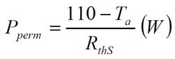

…..[R3-3]
where:
- Ta = ambient temperature in °C and
- RthS = thermal resistance of the solder joint, i.e., its temperature rise in K/W
- Pperm = permissible power.
Information about thermal resistance of the solder joint of standard components applies to soldering conditions for normalized test board patterns.
Solderability is vital for a successful result. The user should use a wetting balance and international standard requirements at inspection. The end caps of MELFs sometimes have been difficult to solder. Metal glaze MELFs with metallized terminations generally have a better solderability.
At gluing or staking check that the termination metal really ”wets”.
R 3.10.5 Failure modes
The weakest point of an SMD is the terminations and solder joints that break after sufficient temperature changes. Good components should stand at least 100 cycles between temperature limits. Applications like modern car electronics have forced the requirements up to some 1000…10 000 temperature cycles.
Except for failures resulting from open mode in connections and solder joints there always are failure modes typical for corresponding hole mount types.
Table R3-7. SMD: CHIP & MELF

R 3.11 RESISTOR NETWORKS
By a network we mean several separate or mutually connected resistor elements collected in a common casing and supplied with terminal leads to each element. Usually the elements have the same resistance value but different values may exist, for example a number of R1 and R2 connected in a ladder pattern that gives a certain voltage division.
In hybrid manufacturing the customer himself applies the resistor elements in a desired casing.
R 3.11.1 General comments
Resistor networks are manufactured both for hole mount and as SMDs. Most parts are manufactured in thick film but thin film as well as metal foil types have a good market.
Discrete SM components may be mounted in the network package. But usually the planar substrates are screen printed with a network pattern either with a metal powder paste that is fired to metal glaze/thick film. Or metal foils are glued to the planar substrate or metal films of NiCr or Ta2N are vaporized or ion implanted – sputtered – on the substrates. The thick film is laser trimmed to the desired resistance value by cutting a track in one of the long sides of the film. However, just as with the discrete chips improved manufacturing technology begins making this laser trimming unnecessary. The other films are designed to a serpentine pattern which reduces the inductance of the element. The metal foils get their pattern by a chemical etching process or by means of the cleaner ion beam etching. The thin metal or metal oxide films are applied through a mask to desired shape.
Just as the chips the resistor element films are protected by a glass coat or sometimes a tantalum oxide coating.
R 3.11.2 Designs
DIL (sometimes DIP) stands for Dual-In-Line respectively Dual-Inline Package (Figure R3-15). The number of leads varies; most common are 14, 16 or 18 leads.
SIL or SIP means Single-In-Line respectively Single-Inline-Package. This network requires less surface but a higher building profile. It exists in the profiles 8 and 5 mm. The latter is most popular. A common number of leads are 4, 6, 8, 10 or 12 (Figure R3-16).
SM networks exist in many different designs. Some are shown in Figures R3-13 and –14. . If the application implies considerable temperature changes examples like those in Figure R3-13 should, due to their lack of flexible leads, be mounted on ceramic substrates.
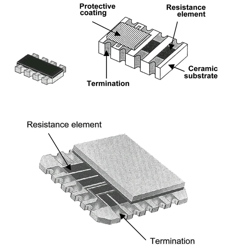

Figure R3-13. Cutaway views of two SM networks: on top resistor array with 4 elements in a rectangular chip, at the foot a network on chip carrier (CC) in JEDEC package.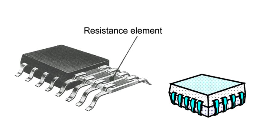

Figure R3-14. SM network, DIL, SO package and “Gull-Wing” lead bending together with a case 4×5 leads and “J-hook” bending.
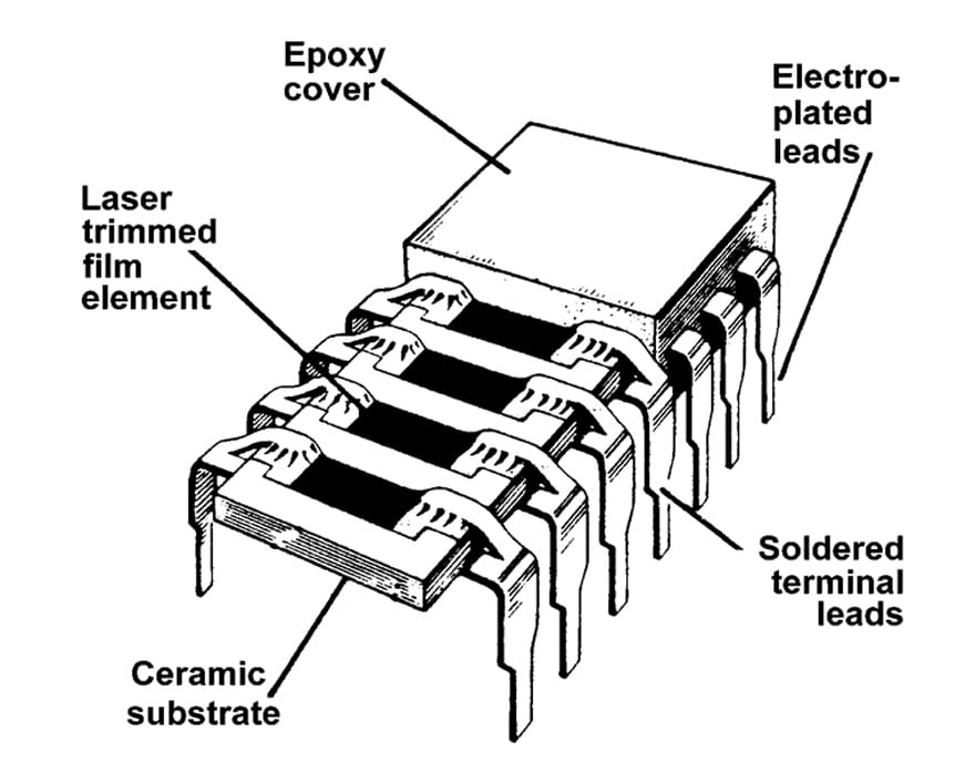

Figure R3-15. Cutaway view of a typical DIL network with 7 pairs of leads and 7 resistor elements.
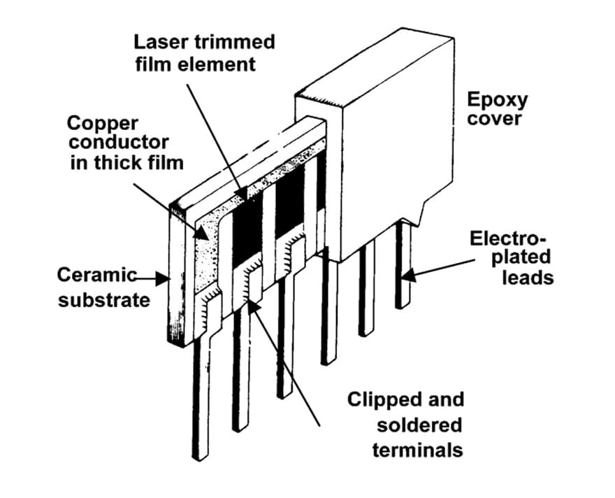

Figure R3-16. Cutaway view of a typical SIL network with 6 leads and 5 resistor elements connected to a common terminal.
Of all requirements that have to be specified and checked there is one that is of particular interest: The coplanarity , i.e., the mutual planarity of the leads relatively to a reference plane. If this measure is not met – d in Figure R3-17 – some leads will be suspended in the air at soldering to the substrate. The measure is exemplified by the gull-wing shape but applies as well to the J hook design.
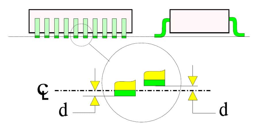

Figure R3-17. Coplanarity = measure d.
R 3.11.3 Configurations
The electrical circuit can be arranged in an infinite number of ways. Usually the resistor values are mutually equal. Sometimes they are bussed (common neutral), sometimes they are arranged separately. Figures R3-18 to R3-23 show examples of the most common configurations.
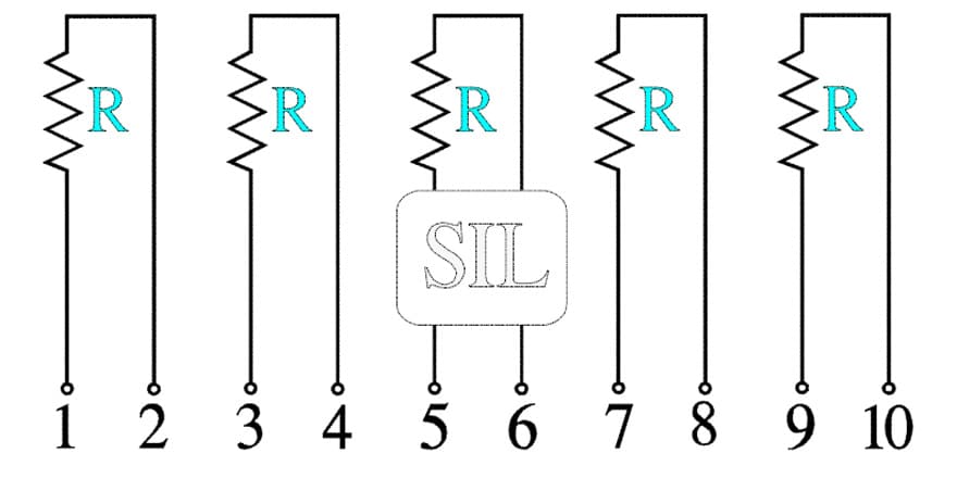

Figure R3-18. SIL network with separate R.
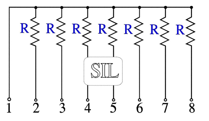

Figure R3-19. SIL network with common terminal.
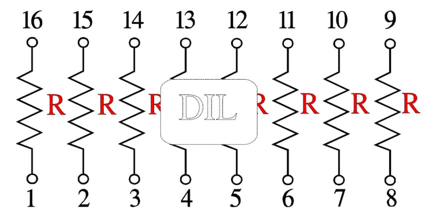

Figure R3-20. DIL network with separate R.
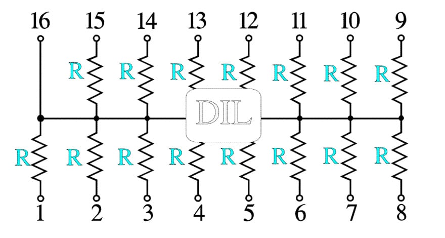

Figure R3-21. DIL network with common terminal.

Figure R3-22. SM network with separate R.

Figure R3-23. SM network with common terminal.
R 3.11.4 Characteristics
In the first place the characteristics of the networks are determined by the resistor material that rules the TCR and the absolute tolerance. Because the elements included belong to the same manufacturing batch their parameter distribution is much more limited than that of the total production. This enables an additional kind of specification that often is used with precision components: the resistance ratio or relative tolerance and the TCR tracking. The concepts are illustrated in Figures R3-24 and –25.
In order to understand the resistance ratio concept better we should recollect how the absolute tolerance is constructed. If the actual resistance is called R and the nominal resistance Rnom, the ratio R/Rnom should be within the tolerance limits. With the relative tolerance, however, we mean a comparison of the different element resistances, Rr, with a reference element, Rref, in the network. Rref usually is the first element in the schematic. The ratio Rr/Rref is called the resistance ratio accuracy, ratio tolerance (or relative tolerance) and is expressed in percent. It is a comparison of magnitude and therefore is given without a sign. If the element values of the network are distributed as in Figure R3-24 we realize that the largest spread will occur if Rref = Rmin and Rr = Rmax. Thus the resistance ratio accuracy, Rratio, shall fulfill the condition (Rmax – Rmin)/Rmin ≤ Rratio.
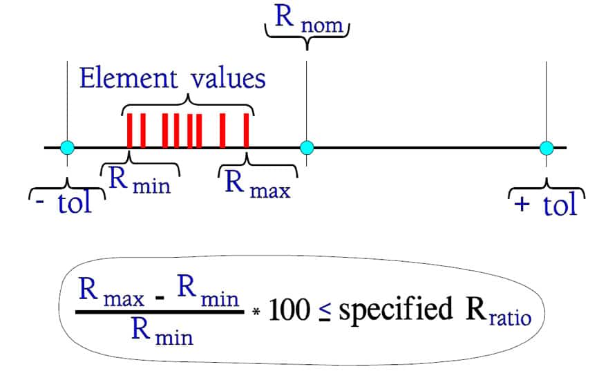

Figure R3-24. Reciprocal tolerance or Resistance Ratio, in percent.
The resistance ratios may range over 0.2 to 2 % for the thick film networks and between 0.05 and 1 % for the thin film networks.
The TCR tracking, i.e., the reciprocal TCR differences between the elements, is illustrated in Figure R3-25.
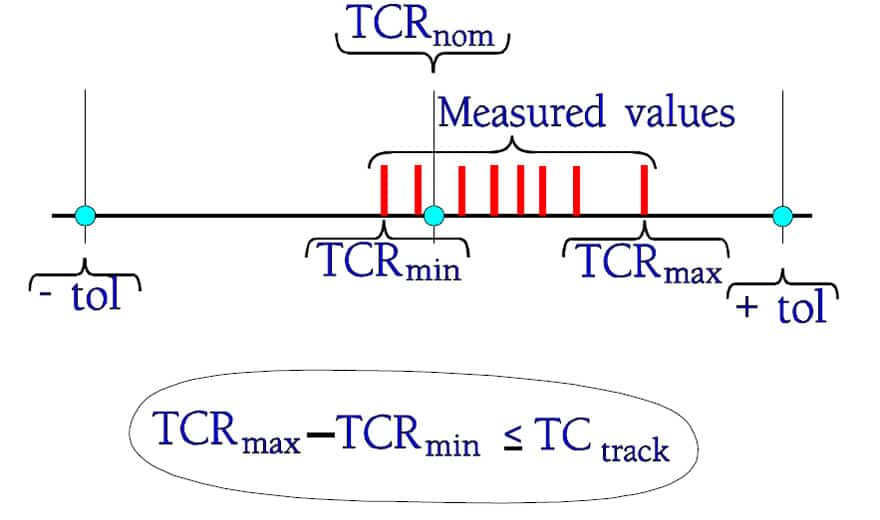

Figure R3-25. Reciprocal TCR difference or TCR tracking.
In practice the following rule of thumb often applies: TCRtrack ≈ ½ x TCRabs where TCRabs means specified absolute TCR.
TCRtrack for the thick film networks usually lies between 10 and 50 ppm/°C and for the thin film networks between 0.5 and 10 ppm/°C.
R 3.11.5 Failure modes
Soldering risks
Terminations with the usual pitch 0.1″ (2.54 mm) are subjected to a mutual thermal influence at soldering. For SM networks there will in addition be the closeness to the substrate and the solder pads. Thus, networks run an increased risk of melting internal solder joints. Even if they will solidify after the soldering process there always is a risk of resulting dry joints. Usually this problem is avoided by specifying use of an internal solder with a melting point well above that of the external solder alloy.
Mechanical weaknesses
The ceramic substrates used often are relatively long and thin. Thermal and mechanical shocks as well as vibration may cause cracks in the ceramic under resistor elements and terminations and result in open modes that in the worst case are intermittent and temperature dependent (the nightmare of trouble shooting). Through hole mounted SIL networks run an extra risk of mechanical damage (if somebody, for example, wants to reposition a network that leans after soldering!).
Mechanically exposed designs sometimes are molded in epoxy, foamed plastic or equivalent. Even if the component surfaces are covered with a mould release agent that is in-
tended to prevent the molding compound to get hold of the components due to shape changes during the hardening process it doesn’t solve the problem with, for example, SIL networks. They are very easily exposed to unsymmetrical side forces that may crack the ceramic substrate.
Table R3-8. RESISTOR NETWORKS

R 3.12 INTEGRATED RESISTORS
In electronics the following trend is prevailing. Working voltages are becoming lower and lower and operating frequencies increase at the same time as downsizing is a key word when delay of electric signals between the active components has to be reduced. The discrete passive components are also becoming smaller and smaller and the component density on the interconnecting substrate increases. This will cause an increase in production cost and failure risk at the same time as the probability of crosstalk grows due to unexpected parasitic capacitances and stray inductances. One step to solve these problems is the use of resistor networks. Next step is to integrate passive components in the printed circuit boards.
On ceramic boards integrated components are no novelty. Integrated resistors and capacitors are common in thick film and thin film circuits. The sheet resistivity of thick film resistors usually ranges from 10 Ω/square to 1 MΩ/square . Values down to 0.5 Ω/square and up to 1 GΩ/square are, however, quite possible. Generally one prints with a width of 0.5 to 1 mm (20 to 40 mils). Then sheet resistivity and element length (number of squares) determine the wanted resistance.
There are now thick film materials available that can be screen printed on polymeric substrates.
In recent years another method of integrating resistors is introduced that is called buried resistors technology. It is intended for large scale production and works with polymeric substrates on which are printed laminates that consist, at the bottom, of a resistive alloy and, on top, of an electrically conductive copper film. The art work of the resistive elements and their terminals are produced by means of photoplot and etching. The resistive film consists of a nickel phosphorus alloy with sheet resistivities of 25 or 100 Ω/square and corresponding thicknesses of 0.4 and 0.1 mm (16 and 4 microinches). By arranging a number of such squares to a bar or serpentine geometry one can create resistance values of hundreds or thousands of ohms. A width may range between 0.2 and 2 mm (8 and 80 mils).
ABC of CLR: Chapter R Resistors
Non-Wirewound Resistors – Carbon, SMD and Resistor Network
EPCI licenced content by:
[1] EPCI European Passive Components Institute experts original articles
[2] CLR Passive Components Handbook by P-O.Fagerholt*
*used under EPCI copyright from CTI Corporation, USA
![]()
This page content is licensed under a Creative Commons Attribution-Share Alike 4.0 International License.

see the previous page:
< Page 7 >
see the next page: