

R 3 NON-WIREWOUND RESISTORS
R 3.1 OVERVIEW
Non-wirewound resistive elements may be produced and arranged in a lot of different ways. We shall present the following types, differentiated by constructional material or specific design:
R 3.2 Film resistors, in general
R 3.3 Metal film / thin film
R 3.4 Metal foil
R 3.5 Metal glaze/thick film
R 3.6 Metal oxide /”metox”
R 3.7 Carbon film
R 3.8 Carbon composition
R 3.9 Conductive plastic.
R 3.10 SMD
R 3.11 Resistor network.
R 3.2 INTRODUCTION TO FILM RESISTORS
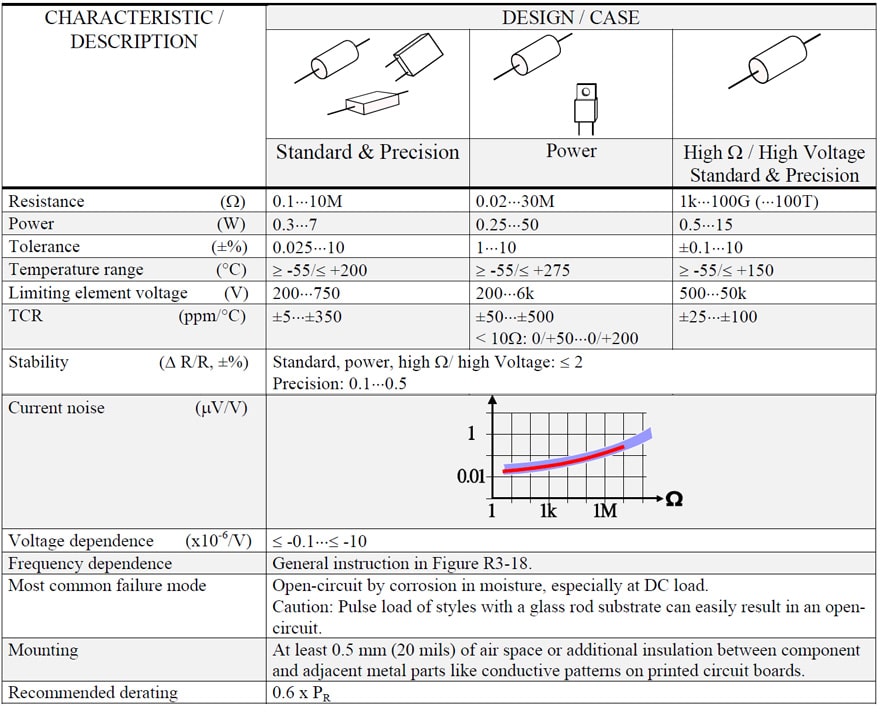
Film resistors are built either on cylindrical rods or on planar substrates. Usually the material in the rods and substrates is ceramic in the state of aluminum oxide (alumina), but glass may occur. Hollow cores exist but are more and more abandoned when sizes are becoming smaller. This design suffers also from drawbacks: the construction is more fragile and the heat dissipation is poorer than that of a solid core.
R 3.2.1 Hole mount
A typical film resistor is shown in Figure R3-1.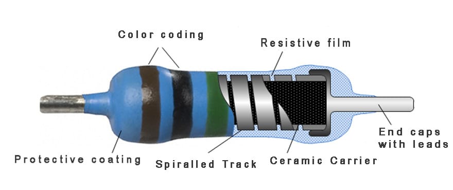

Figure R3-1. Cutaway view of film resistor.
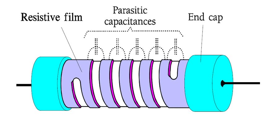

Figure R3-2. Schematic of a spiraled film resistor.
The film of the cylindrical rods thus are cut in a helical track to a long path, usually with a laser. A more stylized sketch is shown in Figure R3-2. The pitch of the helix track can be varied in order to increase the resistance of the film. For thick films an increase of up to 150 times, for carbon and metal films up to 1000 times or even more.
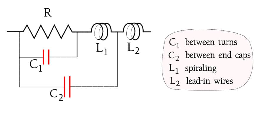
As indicated in the figure a stray capacitance is developed between the turns. Because the turns also constitute a coil the resistor will get a certain inductance. All in all the spiraling produces a frequency dependent impedance where the capacitance is dominating. The conditions are illustrated by the Figures R1-15, R1-16 and R3-3.
Film resistors may be approximately classified as follows:
- values < 100Ω are inductive.
- values between 100Ω and 470Ω are practically true resistive.
- values above 470Ω are capacitive.

Fusible and flameproof resistors
A strong overload of carbon and metal film resistors will lead rapidly to an open circuit that in most cases is accompanied by a build-up of smoke, glow or even fire. Some manufacturers have developed designs that burn off within certain limits. They are called fusible resistors. The open-circuit conditions are defined in particular power-time diagrams. The limits still must be regarded as “broad”.
If coatings and casings are used that don’t generate or sustain a fire, we talk about flameproof resistors. The drawback with these casings in past was partly an impaired environmental protection and partly a troublesome environmental disadvantage from a recycling viewpoint, since they often contain bromine compounds. The modern flameproof resistors has replaced the bromine based fire retardants by a metal oxide compounds. Check with manufacturer datasheets.
Chips and networks
Film resistors also exist as discrete chips or in so called resistor networks where they are collected under a common housing. We will deal with these components separately in section R3.10 and R3.11.
R 3.2.2 Load chart Nomogram
The connection between stability, operating time, temperature, power and resistance usually are shown in particular nomographic load charts. Figure R3-4 shows such a diagram for a sample film resistor. The example reveals how an 1 kΩ resistor working with 0.24 W at an ambient temperature of 80 °C gets a Hot Spot temperature of approximately 137 °C which after 10 000 hours operation produces an expected resistance change of approximately 0.4%. Such a modest change indicates a considerable derating of the nominal power that very well could have been 0.4 or 0.5 W in this example.
Consequently a nomographic load diagram corresponds only to one type and size (power).
In the nomograph example below you shall start at the actual power on the load axes and draw a horizontal line to the right to the parameter of actual ambient temperature. From that point of intersection you draw a perpendicular line that crosses the axis for actual Hot Spot temperature, and continue to the parameter of actual resistance. There you continue horizontally to the parameter of estimated time of operation. From this point of intersection you then continue 90° upwards to the axes marked with the corresponding calculated resistance change.
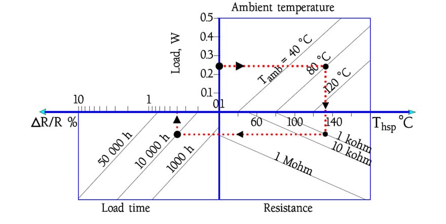

Figure R3-4. Nomographic load diagram for a fictitious film resistor.
R 3.3 METAL FILM / THIN FILM
Today the most dominant type of resistor is the metal film. Sometimes it is called thin film. From the beginning precious metals or resistive alloys were evaporated in a vacuum process and evaporated on ceramic rods. But the TCR specifications especially were hard to fulfil (TCR = temperature coefficient of resistance). Stability and TCR accuracy took a leap forward when one passed to metal ion bombardment of the rods (so called sputtering). Today all the techniques have been developed and refined.
The evaporation technique works both with a vacuum process and a chemical volatility process. Sputtering and ion implanting have become synonymous concepts. The technical progress today motivates manufacturing of high precision resistors. We talk about the third generation of metal/thin film resistors.
Common film alloys are nichrome (CrNi) or tantalum nitride (Ta2N), often with additives of aluminum (Al), silicon (Si) or titanium (Ti). The tantalum nitride has very fine low noise characteristics and is superior in hi-fi applications. Generally, metal film resistors keep noise down by means of laser spiraling that properly utilized produces even tracks free from irregularities. Noise is discussed in section R1.9.
Occurrence of non-linearity – distortion – is mastered by measurement of the third harmonic distortion and automatic screening, where failing parts not meeting stated requirements are removed from the lot.
Distinctive of the metal films is their thin layers – 50…5000 Å or, 0.005…0.5 μm (0.2 …20 microinches). The thinnest films correspond to the highest resistance values where the film starts approaching molecular thicknesses and to some extent deviates from the noise-free conduction capability of metals. Thus the noise is increasingly greater in the high resistance range. Films thinner than 350 Å should be avoided in noise sensitive designs. Another reason for avoiding them is their extreme sensitivity to moisture related electrolytic corrosion, especially if the film consists of a chromium-nickel alloys. Since the film thickness is not stated in the data sheets we may obtain a certain guidance of where the film is getting too thin for high-reliability applications by dividing the manufactured maximum value by 10. Then choose from several serious manufactures the highest manufactured value of the size in question. If the maximum value is, for example, 15 MΩ this rule of thumb gives an upper limit value of 1.5 MΩ. If the application is a dry room environment without large temperature variations (no risk of condensation) and low noise requirements we may use considerably higher resistive values. But still we should, both for reliability and above all availability reasons, take care not to use the highest manufactured maximum value.
Check with other serious manufacturers where their maximum values are and purchase a little bit below the lowest maximum value.
Also, the relatively thickest films are thin and corrosion disposed in moisture, especially if they are working with DC loads. A good encapsulation therefore is necessary. US MIL components exist with hermetic seals but they are relatively expensive. Epoxy/plastic molding does not always offer the same good protection as lacquered coverings, at least not if the lacquer is applied in several thin layers. Farthest in there are one or several – often transparent – coatings of lacquer followed by several layers of colored lacquer. Here the Europeans are far ahead. Duplicated production of cheap standard components with multilayer lacquered coverings probably will come rather close to optimum with regard to price and quality.
Another risk zone for metal film resistors is the ESD – electrostatic discharge. The closer the tolerances, the more important is part protection against ESD.
Finally, metal film resistors are sensitive to power pulses. The power will warm up the thin resistance track very rapidly. Consequently also short pulses may lead to a risk of burning-off or too high temperatures that may hazard the stability. Conservative recommendations talk of maximum 2 x PR where PR stands for rated power. At all events we should not exceed 4 x PR even if the mean power is within specified limits. Single pulses may be much higher but we have to inquire into every particular case: type, manufacturer, value, environment…
R 3.3.1 Low ohmic designs
Values below 10 ohms previously have been manufactured so that the ceramic rods are plated with a resistive alloy, in a bath or a burning process, or by electroplating. The plated layer then will become proportionately thick – between 1 and 5 μm (0.04 and 0.2 mils) – and will have a very good pulse power capability. But tolerances and TC values will be poorer. In the lowest resistance values there is no spiraling which will improve the pulse capability further.
Today some manufacturers have succeeded in producing low ohmic resistors down to 0.1 ohm with the sputtering technique. This eliminates the plating technique difficulties with TCR and tolerance but impairs the pulse capability.
R 3.3.2 Power and precision types
If we load a conventionally power rated metal film resistor with a higher power the temperature will raise and this in turn will decrease stability. Thus power resistors in metal film often have the tolerance ±5% in the E24 series. Alloys and lacquers have been chosen in order to endure higher operation temperatures.
If we go in the other direction and reduce the power – derate – and, moreover, lower the maximum permissible ambient temperature, we get a very stable resistor. IEC 115-5 divides in that way the same sizes in different stability classes, from 0.5 to 0.05 %. It’s the same philosophy as behind Figure R2-9 for precision wirewound resistors. High stability resistors can be worth producing in fine tolerances and TC values. Thus precision resistors of the market are characterized by a low power rating, fine tolerances, low TCR values and a high stability. Note, however, that TC information sometimes is connected to restrictions in the temperature range. The finer the TC, the more narrow the temperature range.
In order to increase the stability further, high precision components are subjected to aging processes where one already under the manufacture releases prospective changes.
R 3.3.3 Linear PTC designs
If we choose metal film alloys that bring out the positive TC of the metals – positive temperature coefficient, PTC – we get relatively linear PTC resistors. Values between +2000 and + 6500 ppm/°C are offered. Just as for the wirewound counterparts the resistance range is limited upwards.
R 3.3.4 Mounting
At least 0.5 mm air space or additional insulation should separate the resistors from adjacent metal parts, for example conductive patterns on printed circuit boards.
R 3.4 METAL FOIL
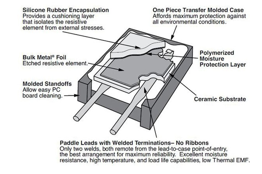

Figure R3-5. Cutaway view of metal foil resistor.
Within the metal film technology there is a particular type of precision resistor made by metal foils, by the inventor, Vishay Intertechnology, called Bulk metal foil. These resistors exist both in axial and radial designs for hole mount, further as SMDs, networks and power styles, finally also in PTC designs.
Figure R3-5 shows a principle cutaway view of a foil resistor from the manufacturer Vishay. The etching pattern is not shown.
The coefficients of the thermal expansion of the resistance alloy and substrate are different. When the alloy foil is firmly attached to the ceramic substrate in a unique way it results in a compressive stress on the alloy when temperature increases. The resistivity of the alloy versus temperature changes is matched with variations of the resistance of the alloy with stress. In other words, by this method the physical expansion behavior of the foil is forced to follow the considerably lower expansion or shrinkage movements of the substrate at temperature changes. This results in a foil with excellent stability and TCR characteristics. The construction also results in outstanding characteristics of thermal electromotive forces and voltage coefficients.
The foil then is etched to a serpentine or labyrinth pattern, either by means of a photo resistive film, mask and chemical etching (photo lithography), or by means of a guided ion beam. Particular, not mold encapsulated styles, can be bought together with trimming tools. By scribing an open-circuit in particular conductance paths the resistance value may be trimmed to extremely fine tolerances. The patterns eliminate much of the inductance that burdens spiraled components.
Since the foils have thicknesses of more than 2.5 μm (0.1 mil) they have excellent pulse resistant characteristics. They don’t suffer from the extreme corrosion sensitivity of thin films either. The disadvantage is that the maximum resistance of metal foil styles will be limited (See Table R3-1).
The most common failure mode of metal foil resistors is open-circuit in contact joints after temperature changes or of shifts in resistance as debris or weak spots in the resistive path burn out.
Table R3-1. METAL FILM & METAL FOIL RESISTORS[1]
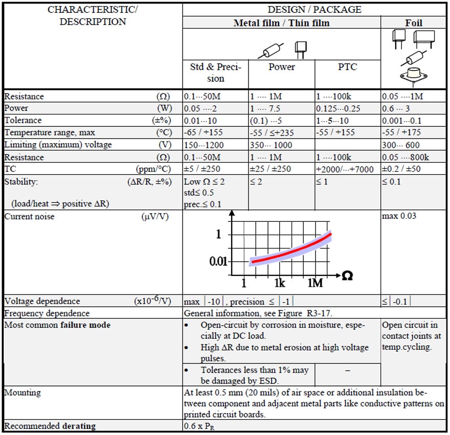

[1] SMD, see Section R3.10.
R 3.5 METAL GLAZE / THICK FILM
If we screen print a paste of finely scattered metal particles (for example ruthenium, ruthenium oxide, rhodium, palladium, tantalum-tin) together with glass powder on a ceramic substrate and fire the film until the glass melts, we get a resistive film from some μm up to 25 μm (1 mil) of thickness, a so called thick film or metal glaze. The substrate has to be chosen with great care in order to constitute an integrated part of the melted glass powder. A variant of thick film exists in some potentiometers under the name of cermet. Actually it is a manufacture connected film that first was put on the market by the manufacturer Beckman Industrial. Today the name cermet is generally recognized.
The film is very environment resistant and has surface resistivities up to 1 MΩ/square, which allows high resistance values in small chip sizes. Here the thick film meets with its dominating application together with its existence in networks. Axial through hole mounted components are manufactured almost exclusively as high ohmic/high voltage types. Traditional high ohmic resistors in the 100-MΩ range of carbon composition, carbon film or metal oxide designs generally with advantage can be replaced with metal glaze resistors.
After the firing cylindrical bodys are spiraled as shown in Figure R3-1 and R3-2. Plane surfaces are laser trimmed to exact values. The tolerances usually are situated between 1 and 10 % and the TCRs between ±25 and ±300 ppm/°C. The closest TCR, ±25 ppm, deserves certain caution because of the risk of drift outside the specification limits.
The conduction mechanism in the metal glaze/ thick film consists of contacts between small metal granules. This leads to considerably more noise than in genuine metal film resistors. Furthermore the user should be careful with strong pulse loads, at least in the k range. They might give permanent resistance changes due to damaged contact points.
Another phenomenon that characterizes thick film materials more than pure metals is non-linearity. The thick film with its complicated conduction network and countless contact spots suffers from non-linearity at relatively low resistance values. Following diagrams show the difference between thick film and metal film materials in two SMD styles: a metal film “MELF” and a thick film chip.
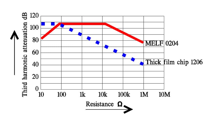

Figure R 3-6. Examples of third harmonic attenuation in different resistor materials.
Table R3-2. METAL GLAZE / THICK FILM RESISTORS

R 3.6 METAL OXIDE (“METOX”)
The metal oxide resistors have increasingly been replaced by metal film resistors. But, they still have a market, above all in the high ohmic-high voltage range. Precision designs exist in all resistance ranges.
There are different ways of producing resistive metal oxide films. If we heat ceramic rods in a vapor of stannic chloride we get a coating of stannic oxide with good resistive characteristics. The thickness is approximately 1μm (0.04 mils). If we instead use glass that in a hot state is extruded in a stannic chloride vapor, it will result in a film of stannic oxide that is integrated with the glass to form an environment resistive resistance film. It will withstand several hundred per cent overload with good stability. On the other hand these resistors are extremely sensitive to stronger power pulses, also of short duration. Another way to produce metal oxide films is to first apply a metal film on the rods and then oxidize the film in an oxygen gas.
Normally the rods are spiraled in a conventional way. The lead pattern, however, can be formed in an inductance-limiting serpentine pattern as shown in Figure R3-7 from the manufacturer Caddock Electronics, Inc.
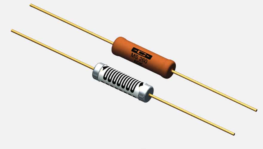

Figure R3-7. Inductance limiting serpentine pattern burnt on a cylindrical rod. Caddock Electronics, Inc.
The metal oxide film has excellent noise characteristics, next to metal films the best. Unlike other films it does not run the risk of being oxidized at higher temperatures.
It already is oxidized. Thus, in certain power resistors Hot Spot temperatures up to 275 °C are permitted. But the user needs to check with the manufacturer’s data sheet about how much the chosen type can stand. It varies. Sometimes the power types are supplied with cooling plates integrated with the housing.
Certain types of metal oxide films also are suited for high voltage or high ohmic types, the latter in values up to at least 100 GΩ.
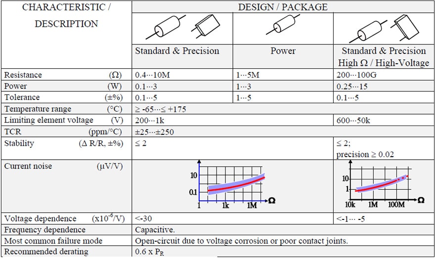
Table R3-3. METAL OXIDE (“Metox”) RESISTORS

ABC of CLR: Chapter R Resistors
Non-Wirewound Resistors – Metal Film, Foil and Metal Oxide
EPCI licenced content by:
[1] EPCI European Passive Components Institute experts original articles
[2] CLR Passive Components Handbook by P-O.Fagerholt*
*used under EPCI copyright from CTI Corporation, USA
![]()
This page content is licensed under a Creative Commons Attribution-Share Alike 4.0 International License.

see the previous page:
< Page 6 >
see the next page: