by Stephen Oxley M.Eng C.Eng MIET, TT Electronics UK
presented by S.Oxley at the 2nd PCNS 10-13th September 2019, Bucharest, Romania as paper 1.3.
Abstract
Film resistor technologies have come a long way since metalised glass and cracked carbon films were first offered over eighty years ago as alternatives to the bulk material approaches of wirewound and composition. Metal oxide emerged in the 1950s as a more stable film and was widely applied until ceding ground to metal film for precision and thick film for high power uses. Both of these technologies were then employed in the emerging SMD chip format. This point was reached over thirty years ago and is largely reflected in today’s film resistor offering. However, it would be a mistake to think that nothing is changing in the world of film resistors.
This paper identifies three drivers of continued evolution and outlines some of the developments which are being made in response. The first driver is the imperative to reduce environmental impact and is felt through legislated regulation and, indirectly, consumer pressure. Following this is continued expansion of the safe operating area, pushing back on the electrical rating limits which constrain miniaturisation of analogue circuits. And finally, rising demands for higher levels of stability and reliability in commercial and industrial applications are being met by the transition of technology developed for space and military applications
Two responses to the environmental driver are identified. The first is the reduction in overall material usage reflected in miniaturisation and the second is the elimination of hazardous substances. In the area of thick film resistors this is seen in the removal of lead oxide from the glasses used in formulating the film material. The extent to which this reduces reliance upon the continued renewal of the associated RoHS exemption is considered.
For the second driver, three electrical ratings defining the safe operating area for resistors are reviewed; continuous power rating, limiting element voltage and pulse energy limit. Each is defined and the results and failure mechanisms of moderate and extreme overloads are presented with practical examples. The dependence of these three ratings on the materials, dimensions and geometry of resistive components is discussed, with reference to the continuing trends to transfer designs to SMD formats and to minimise footprint area. The current status of commodity thick-film chip resistors with respect to these ratings is then given, and multiple component solutions and their hidden costs are discussed. Existing and new techniques are then presented whereby the three ratings may be extended.
The final driver relating to stability and reliability is leading to the progress of tantalum nitride technology from its high reliability origins into the mainstream of precision resistor applications. The differences relative to alternative materials are examined together with the performance benefits indicated by highly accelerated life testing.
Although the pace of change seems slow when measured against that of semiconductors, and even other passive components, the development of film resistor technology is still continuing in the 21st century.
Driver 1: Mitigating Environmental Impact
Miniaturisation
The environmental impact of component manufacture under given processing conditions is largely a function of the mass of materials consumed per article. This has undergone a long-term downward trend which is set to continue for the foreseeable future, as shown in Table 1. Broadly speaking we see a halving of peak popularity component mass approximately every decade with a suggestion that this rate is showing signs of decline. Unlike Moore’s Law which is becoming limited by hard processing constraints, chip resistor down-scaling is always restrained by the innate requirement to generate heat in operation, and the consequent power ratings required by designers. As resistor ratings descend towards the single milliwatt range, it is likely that this will bring miniaturisation to a virtual stop, albeit a more gradual stop than is anticipated for transistors. Furthermore, it should be noted that the older, larger sizes never become obsolete. Even the 2512 size chip resistor from the 1980s is alive and well, albeit at a very low proportional usage.
| Size Code | 1206 | 0805 | 0603 | 0402 | 0201 | 01005 | Other |
| Year of peak proportional usage | mid 1990s | late 1990s | 2000 | 2010 | 20241 | 20351 | |
| 2019 proportional usage | 4% | 7% | 17% | 33% | 28% | 9% | 2% |
| Typical mass relative to 1206 | 100% | 52% | 20% | 6.0% | 1.6% | 0.78% | |
| Typical number of resistors per gram | 111 | 214 | 555 | 1,850 | 6,940 | 14,230 | |
| Note 1- estimates based upon the time from inception to peak exhibited by larger sizes |
Table 1 Chip Resistor Size Trends
It is recognised that environmental impact is by no means the only driver of this trend, or even the primary one. Clearly that place belongs to the economic imperative for lower unit cost and the functional imperative of enabling smaller end products in consumer mass markets. However, it is worth mentioning here that the environmental benefits, as measured per resistor, are very real and set to continue.
Hazardous Substances
Lead (Pb) has long been recognized as a serious environmental hazard. It has a detrimental effect on the workings of the human central nervous system, and this is particularly acute when children are exposed to it. Based on the findings of scientific research conducted during the 1960s, the presence of lead in petroleum, paints and other household products was phased out over the course of the 1970s and 1980s and further legislative measures gradually saw it eradicated from most aspects of our everyday lives.
The Restriction of Hazardous Substances Directive 2002/95/EC (RoHS) legislated to remove metallic lead from electronic components, along with other harmful constituents such as mercury or cadmium, and replace them with alternatives that did not have such a severe ecological impact. The legislation was brought into effect in 2006, though most suppliers had already conformed to it a couple of years prior to it being enforced. It should be noted though that there are certain exemptions to the RoHS directive – where, at the time of its implementation, no viable substitute could be found.
Among the areas where an exemption would prove to be warranted was in thick-film resistors, and to this day the incorporation of lead oxide compounds into their glass elements is still permitted. Though much more environmentally stable, and thus posing less of an immediate threat, there is still a risk of these toxic heavy metal compounds entering the surrounding environment over time, leaching into groundwater from landfill sites. Due to growing concerns about the huge quantities of electronic waste now being amassed, there is currently renewed pressure to look at narrowing the scope of the existing exemptions and make regulatory guidelines more stringent.
It is important for OEMs to be aware that the current RoHS exemptions that are in place are subject to periodical review. Hence, there will be the potential risk of components that have already been specified into electronic designs to no longer be within the exemption scope. Clearly this could have serious and extremely costly implications for an OEM that fails to be adequately prepared, and this is now leading some to take pre-emptive.
The next review of the relevant RoHS exemption 7(c)-I ‘Electrical & Electronic Components Containing Lead in a Glass or Ceramic Material’ – is scheduled for 2021, and during this review the inclusion of lead oxides in thick-film resistors may be placed under considerable scrutiny. OEMs are calling for components with which they can future-proof their system designs in case RoHS exemption changes are made. Consequently, they will not have to worry about allocating additional time and engineering resources to make amendments further down the line – when there is an imminent deadline.
The removal of the lead oxides from glass in thick-film materials is not simple to achieve, and attempts to do so have often had associated electrical performance penalties1. Research in this area actually pre-dates the original RoHS implementation, but by the mid 2000’s was beginning to yield materials suitable for commodity resistors. Green versions of standard chip resistors have been available for several years, and have been acceptable in less technically demanding cases. However, these have not got close to attaining the benchmarks necessary to address higher end applications. This has recently begun to change with one manufacturer offering a high voltage chip resistor fabricated from “green” thick film materials. This is able to match the ratings of similar parts made from conventional materials but not yet at quite the full ohmic value range or the same temperature coefficient.
Launched in late 2018, TT Electronics’ green high voltage chips (GHVC) are targeted at hybrid electric vehicles (HEVs), industrial automation, clinical medical and home healthcare applications, where they will serve in either high-voltage sensing or circuit protection functions. Though important in all forms of electronic design, the future-proofing aspect will be of particular value in a medical context, as using green components will mean that not only redesign, but also onerous requalification procedures can be avoided.
Early experience shows that by using more advanced materials and implementing a new fabrication process, but not having to make any significant financial outlay on the upgrading of equipment, the migration to a fully lead-free strategy has not represented a major increase in production expenses. Therefore, the price points are effectively the same as with products containing lead oxides. Initially the expectation is, on average, for GHVC pricing to be around 20% higher – though this is expected to drop as volume demands increase and economies of scale start to take effect.
There are some outstanding hurdles for green thick-film materials to clear before RoHS exemption 7(c)-I can be regarded as fully redundant. These include reducing temperature coefficients, which can be up to double those of conventional materials and improving stability to high instantaneous temperature events, which will enable the transition of high surge energy products.
Driver 2: Extending SOA
Introduction
The design of thick-film chip resistors has changed little since their introduction in the 1970s. From specialist beginnings they have become the mainstay resistive element in small signal applications across all product sectors. However, the compact format, which has underpinned their popularity, also places severe constraints on their electrical ratings. This is, in part, the reason why, for resistors, the through-hole format has not disappeared completely.
However, continuing development and deployment of SMD processing results in pressure on component manufacturers to convert as much of their range as possible into the near-ubiquitous chip format. Whilst there will always be limits to this process, recent years have seen innovative chip solutions pushing back the boundaries. With an involvement in thick-film technology stretching back to the 1960s, TT Electronics has been at the forefront of product development in this area.
Defining the Boundaries

The primary rating for any resistor is the maximum continuous power that may be dissipated at a stated ambient temperature (hereafter termed the power rating, Pr.) This is more dependent on PCB track design than is the case for through-hole parts, as thermal conduction rather than convection is the predominant means of heat loss. Standard mounting conditions, which may or may not be stated on the product datasheet, are therefore a condition of this rating.
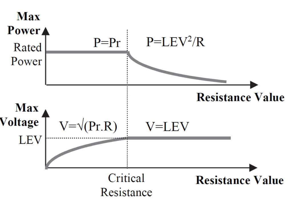
The second rating considered here is the Limiting Element Voltage (LEV) or maximum continuous operating voltage (hereafter termed the voltage rating.) This applies only to ohmic values above a threshold termed the Critical Resistance. At values R below this threshold the voltage is restricted by the rated power to V=√ (Pr.R). The effective maximum power and voltage limits across the ohmic range of a resistor are illustrated in Figure 1.
The third rating relates to the short pulse energy capacity (hereafter termed the energy rating.) For a thick-film chip the energy limit depends on pulse duration and is generally presented as a graph of peak power as a function of duration for single pulses (where mean power is negligible) and for continuous pulses (where mean power = Pr.)

Failure Modes
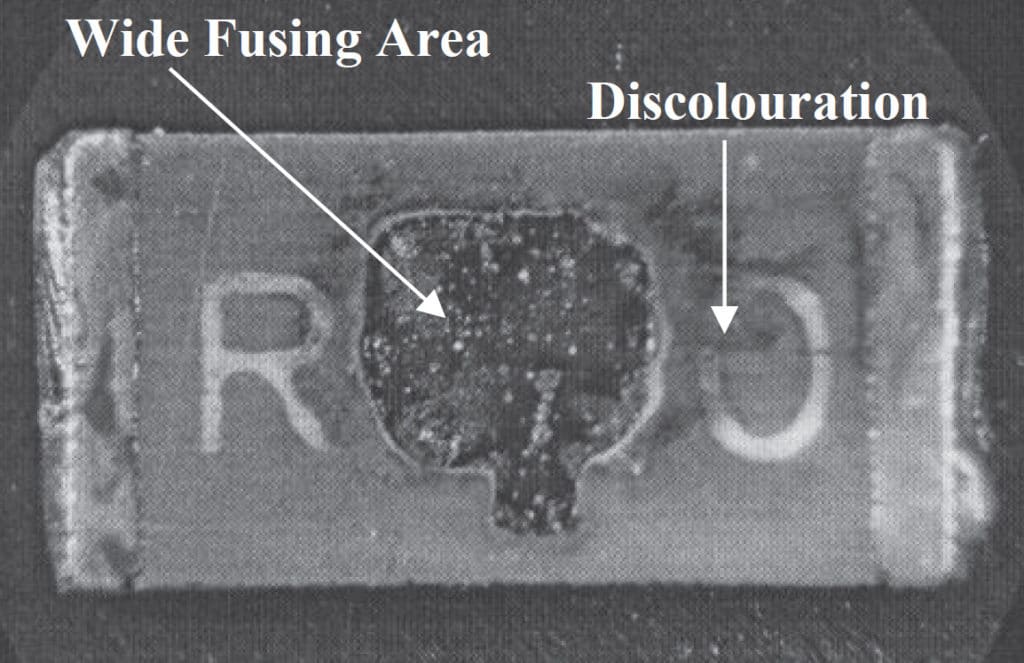
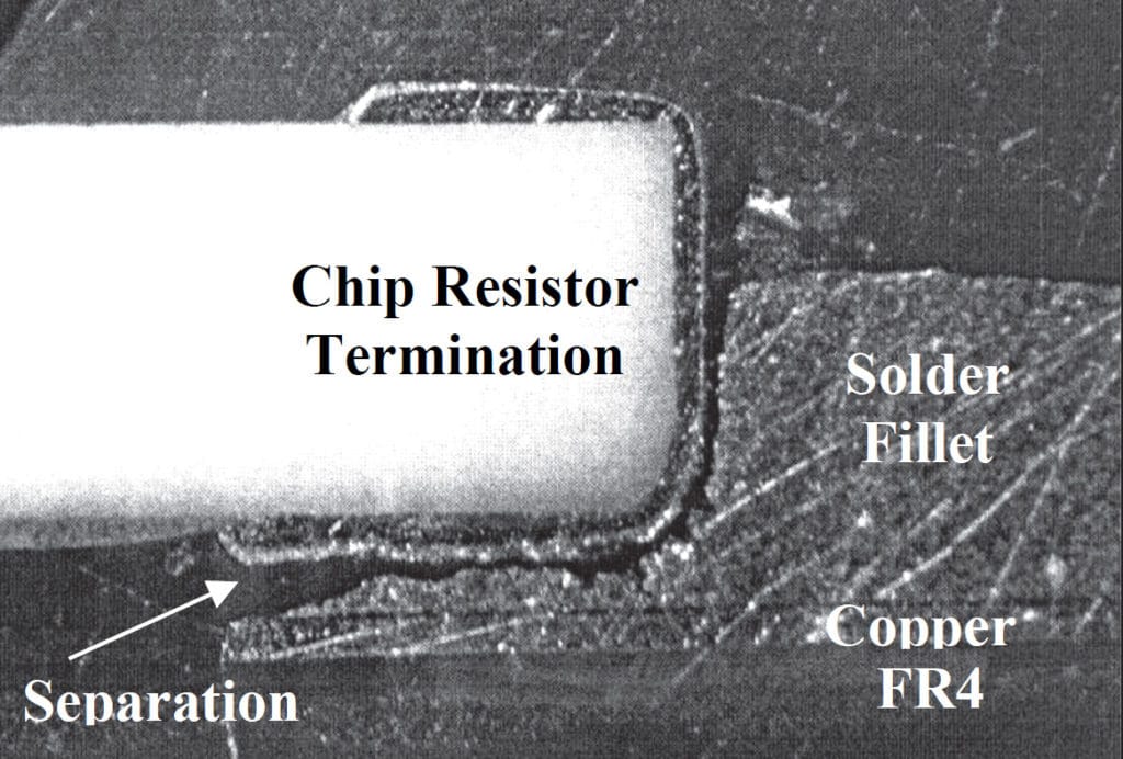
Exceeding the rated power for a limited period is generally acceptable (6.25 times Pr for 2 seconds is typical) but prolonged overload can clearly result in excessive film temperatures. This will lead to value instability, usually in the form of a positive resistance shift. This is due to microcracking in the thick-film material and as it results in higher resistivity hot-spots it tends to be a progressive change. This may be associated with discolouration and degradation of the insulation. In a more extreme case the film element can fuse completely (see Figure 2.) Also the solder fillets can become unreliable, especially if the overload is cyclical in nature (see Figure 3.) Finally, scorching of the PCB and overheating of surrounding components are possible secondary outcomes.

Exceeding the voltage rating can also result in value instability, but in this case the shift is negative. This is due to the creation of new current carrying pathways between conductive particles within the thick-film material in response to excessive electric field strength, resulting in a permanent decrease in the sheet resistance. This is generally a self-limiting effect giving rise to shifts of up to 5%.
Higher voltage overloads will produce electrical breakdown often beginning across laser trim cuts where the electric field strength is greatest. Results range from resistance decrease due to internal leakage and external tracking through to a flashover event with sufficient energy to fuse the element.

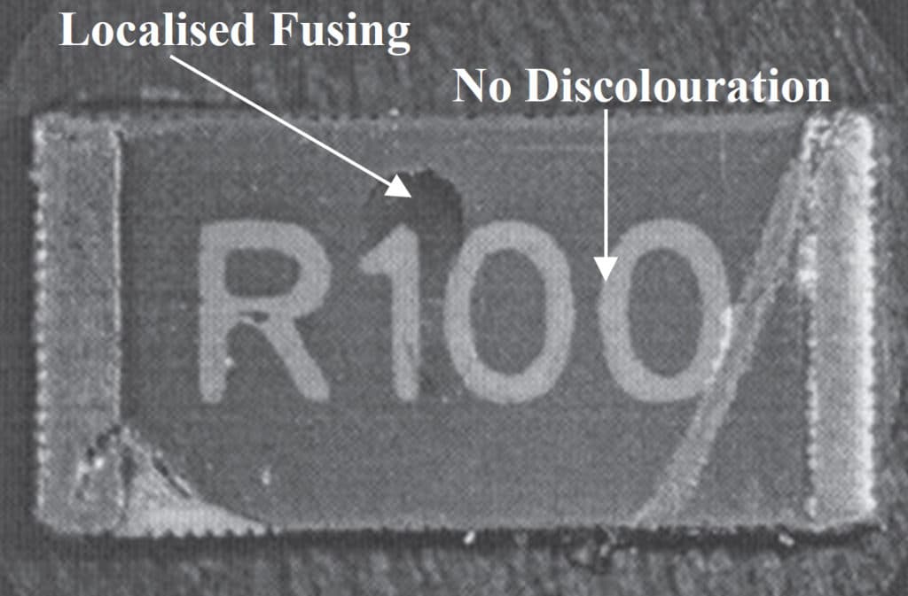
Exceeding the pulse energy limit can result in value increase or fusing as in the case of continuous overload, since the underlying thermal mechanisms are the same. The distinction is that pulse failures result from rapid, localised heating. This means that the effects tend to be more focussed on regions of current crowding at the end of laser trim cuts. Often it is only this limited region of the film that fuses, leaving the remainder of the component and the solder joints unaffected (see Figure 4.)
Limiting Factors
All three of the ratings described here are influenced by the materials, dimensions and geometry of the product. Regarding materials, there is limited scope to improve performance using ruthenium oxide (RuO2) thick-film materials with finer particle size for greater film homogeneity combined with careful process control to eliminate pinhole defects arising from air bubbles at the wet print stage. Furthermore, for low ohmic values, high metal content inks can replace RuO2, and their higher thermal conductivity assists heat spreading [2].
Regarding substrates, using ceramics with high thermal conductivity such as aluminium nitride (AlN) offer obvious benefits against conventional alumina (Al2O3). However, the cost implications restrict the use of such materials to applications such as RF and microwave where very high power densities must be realised and increasing the dimensions is not an option.
This leaves geometry of the resistor element, as defined by printing and laser trimming processes, as the key determinant of performance.
| Rating | Determining Factor | Design Approach |
| Power | Uniformity of film heating | Minimise lateral trim. |
| Thermal impedance from hot spot to PCB | Adjust element orientation. | |
| Voltage | Track length | Use optimised serpentine form. |
| Energy | Active film area & avoidance of current crowding | Maximise print area. inimise trim & shadow area. |
Table 2 Effects of Geometry on Ratings
The relationships between component geometry and the three ratings are shown in Table 2. The design approaches suggested here relate to the design of the resistor element and to the process of laser adjustment and are discussed in detail later in this paper.
Multiple-Chip Solutions
| Chip Size | Power Rating | Voltage Rating |
| 0201 | 50mW | 25V |
| 0402 | 63mW | 50V |
| 0603 | 100mW | 75V |
| 0805 | 125mW | 150V |
| 1206 | 250mW | 200V |
Table 3 Typical Commodity Chip Resistor Ratings
The typical power and voltage ratings of conventional thick film chip resistors are given in Table 3. Typical energy ratings are not given as in most cases the pulse characteristics are not defined on the datasheet at all. Furthermore they may not safely be derived from limited sample testing due to significant batch-to-batch variation in the degree of laser trimming applied.
One approach to realising SMD resistor solutions with higher ratings is clearly to use multiple chips. Provided the spacing is adequate (and this is critical) N chips will provide a power rating of N.Pr. Furthermore, if in series, the voltage rating is also scaled up N times. This can appear to be a low-cost solution when looking only at the material costs, but there are hidden costs, which a designer should also consider.
The first of these is placement cost. Modern SMD placement systems have brought this down to the range of 0.1 to 0.4 eurocents per chip. However, figures based on rated machine speeds should be used with care; the real world speed can often be around half the rated speed, with the real placement cost being proportionately higher [3].
The second hidden cost is that related to quality, and includes inspection, rework and field failure cost increase due to the multiple solder joints. No general figure can be given here as so much depends on the manufacturing environment and product sector, but a designer should take a view of the impact of quality costs on design strategy.
Even with these costs taken into account a multiple-chip solution can look more attractive than a single high-rating chip. But there is finally the cost of the extra space used. This includes not only the material cost of the additional PCB area and associated housing materials but also the opportunity cost related to miniaturisation; how would having a more compact product affect market share?
When all these factors are accounted for there is often a case for a single high-rating chip, especially in designs where:
- Power or voltage ratings are many times those available in commodity parts
- PCB flexing or temperature cycling requirements constrain the use of larger chip sizes
- There is significant value in reducing the solution footprint
- Pulse withstand performance must be guaranteed
Extending the Ratings
Some of the methods used for extending the three electrical ratings of thick-film chip resistors are as follows.
Extending the Power Rating
The peak film temperature may be minimised firstly by ensuring that heat is distributed evenly over the chip surface, and secondly by lowering the thermal impedance to the PCB tracks.

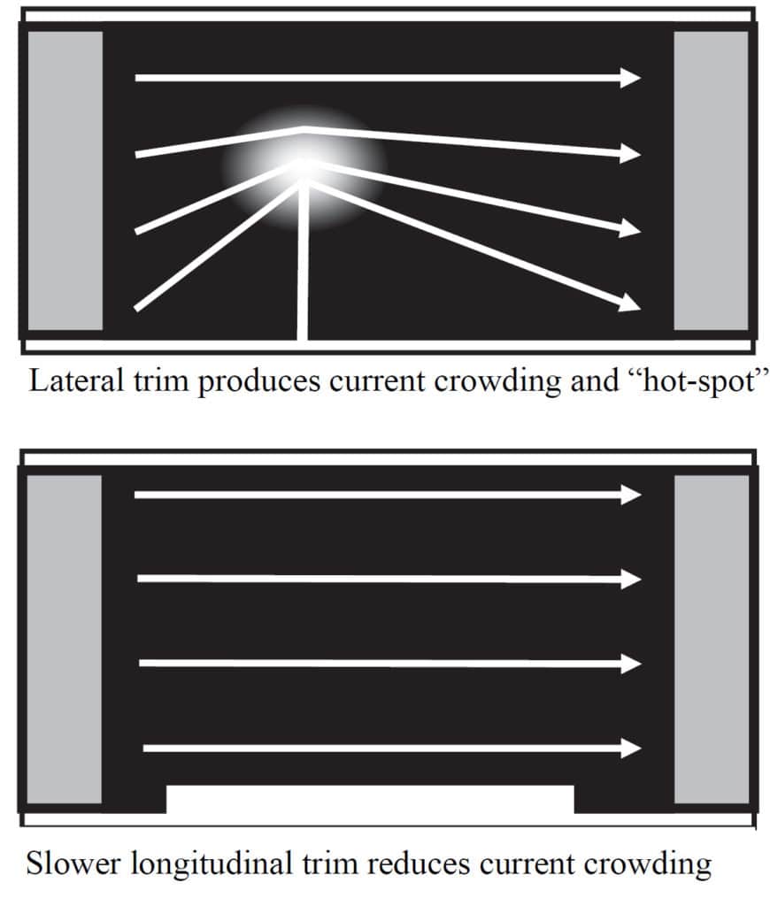
Two trimming techniques are shown in Figure 5; the first is the faster and is employed in commodity chip manufacture. The second is slower but avoids the high temperature peak. It is employed in TT Electronics’ PWC series where it permits a power rating increase of up to 50% for the same peak film temperature of 155°C.
Having spread the heat evenly, the next task is to get rid of it effectively. Depending on the mounting conditions, between 60 and 90% of heat generated is lost through conduction into the PCB copper tracks. The remainder is lost through convection and radiation. This means that the effective power rating of a chip resistor is partly a function of layout design.
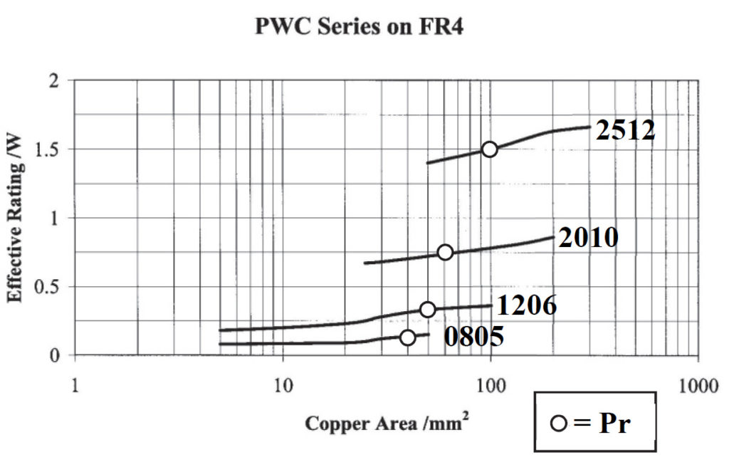
In order to quantify this relationship, chip resistors of various sizes were mounted on FR4 test boards with different areas of copper heatsink in the form of rectangular blocks immediately adjacent to the solder pads. In each case the applied power producing the maximum film temperature rise was found. The results for PWC in Figure 6 show a 15 to 20% variation in effective power rating is possible.
The same study has shown that the lower internal thermal impedance of TT Electronics’ low-value LR series, which results from its thick-film copper terminations, can yield larger variations of up to 100% in effective power rating.
The general relationship between effective power rating and PCB copper area is as indicated in Figure 7. This can be divided into three areas.


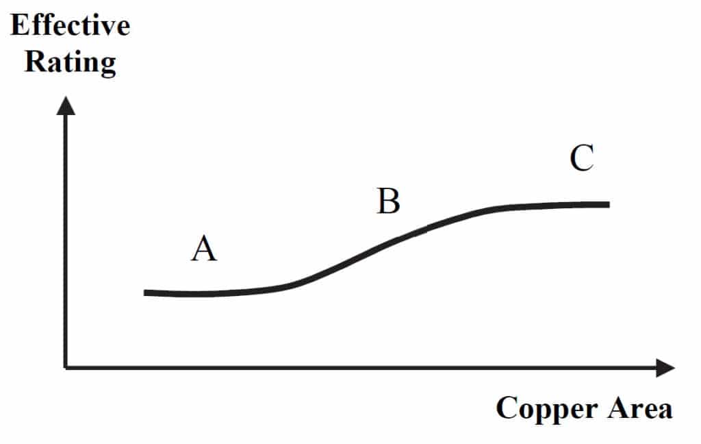
In area (A) there is relatively low thermal conduction through copper connected to the pads and conduction by substrate and convection to air predominate. In area (B) the copper connected to the pads acts as a heatsink to raise the effective power rating. In area (C) further increase in copper area gives diminishing returns as the internal thermal impedance of the chip restricts the rating.

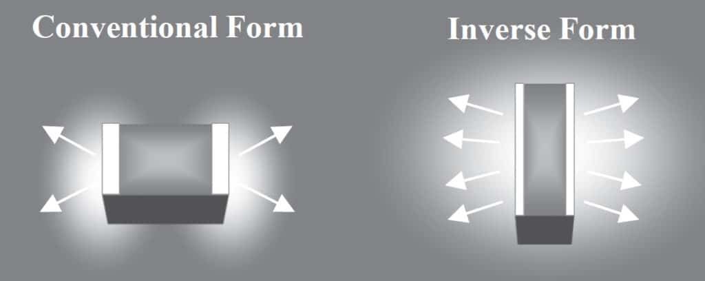
This limiting factor of the internal thermal impedance may be lowered significantly by changing the orientation of the resistor. If the terminations are formed on the longer edges of the chip rather than the shorter edges, the solder joint width is approximately doubled and the maximum distance from film centre to termination is approximately halved. The principle is shown in Figure 8.
This is the basis of inverse form products such as TT Electronics’ SC3 and LRF3W that can achieve a triple power rating over the conventional form (e.g. up to 3W @70°C in a 2512 1W footprint with 300mm2 copper area.)
Extending the Voltage Rating

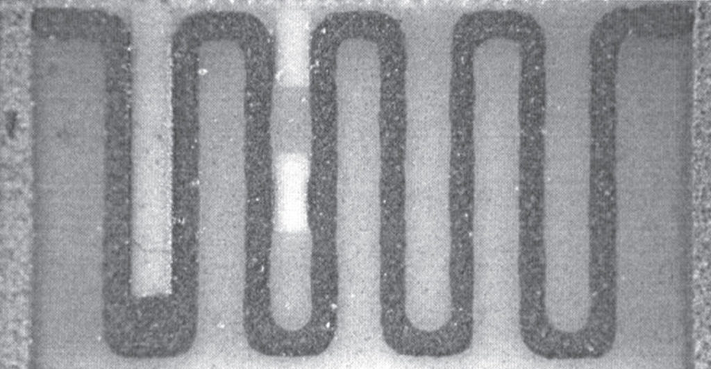
The key to raising the voltage rating is the use of a serpentine track design. This has been used for many years in through-hole high-voltage parts, and is now available in chip products such as TT Electronics’ HVC series. The element layout for the 2512 size is shown in Figure 9. This serpentine form has the twin benefits of achieving a fivefold increase in track length with resultant reduction in voltage stress and enabling the use of lower resistivity inks, which are more stable at high voltages.
This technique allows a chip resistor to be manufactured with a voltage rating of 1kV in 1206 size and 3kV in 2512 size, subject to the layout and environmental factors outlined below.
In practice, a designer is unlikely to use the full voltage rating of the resistor, as the voltage applied between the solder pads will be constrained by minimum creepage and clearance design rules. Clearly, the PCB layout should avoid tracks running between the mounting pads, as this would compromise the voltage rating. A number of environmental conditions also apply if the full voltage rating is to be used. The rating stated applies to operation at sea-level pressure and in a non-condensing atmosphere.
Finally, it is especially important to avoid contamination. This may arise from a number of sources:
- Chemical traces may remain from the PCB manufacture process. Even if the surface is clean, traces may leach out of the substrate when heated.
- An appropriate cleaning process should be used. In particular, if a “no-clean” flux is used, the removal of cleaning may make the process more vulnerable to other sources of contamination.
- Either before or after assembly, handling can introduce ionic contaminants and should be controlled.
In most applications though, these limiting factors still permit considerably higher voltages to be applied than the 50 to 200V limit of commodity chip resistors.
Extending the Energy Rating

The short pulse performance is dependent on active film area. This is the area of thick-film material which develops heat and which alone must absorb it if the pulse is of too short a duration to permit significant heatsinking by the ceramic substrate.
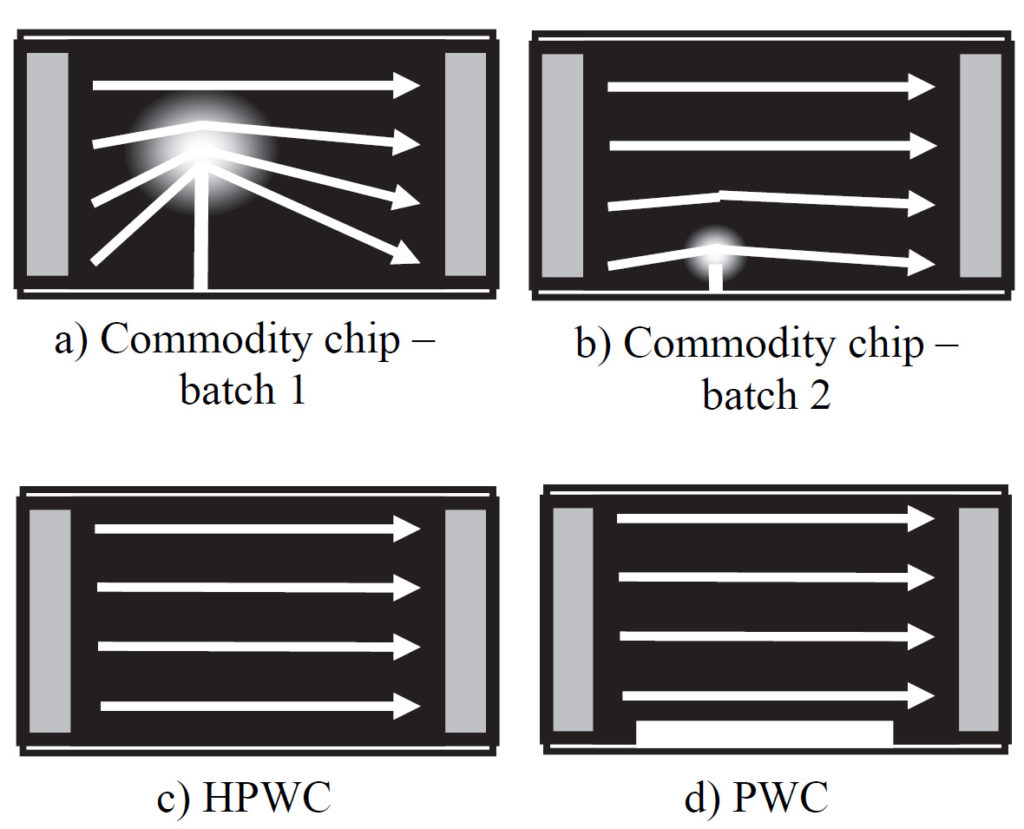
Lateral trimming reduces active film area significantly. This is because, although only a small proportion of the film area is actually removed by the laser cut, the film adjacent to the cut (in the shadow region) has a greatly reduced current density and therefore a diminished contribution to the total energy capacity. Furthermore, the current crowding described above in relation to power rating also produces a hot-spot region under pulse conditions. Because of the wide variation in lateral trim cut length (see Figure 10 a & b), commodity chip resistors have a wide spread in energy capacity. This is important to note, as a part which functions well in a prototype of a pulse application as it is like batch 2 can fail in volume production which includes parts trimmed like batch 1.
The simplest solution is to omit trimming altogether, as in TT Electronics’ HPWC (Figure 10 c). However, owing to the process capability of printing and firing thick-film inks this is only achievable in 5% tolerance, with tighter tolerances being achievable only by means of grading and therefore incurring higher cost due to the limited grading yield.

TT Electronics’ PWC (Figure 10d) employs longitudinal trimming to 0.5% tolerance with only a marginal loss of active film area. It therefore combines the tolerance of a trimmed chip with a pulse performance approaching that of an untrimmed chip.
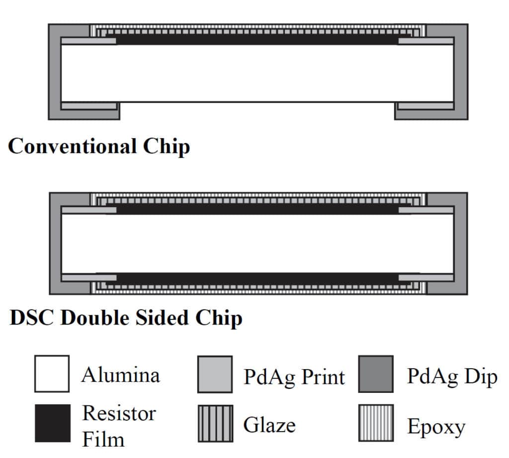
For a more radical solution we need to go back a stage and consider ways to apply a greater area of thick-film material to the chip. TT Electronics’ DSC series doubles the film area by the approach of applying a resistive element to both the upper and lower faces of the chip (Figure 11).

This is combined with the same trimming technique as used is for PWC to give energy capacities approaching those of wirewound resistors of the same footprint, especially at ohmic values above about 10W.
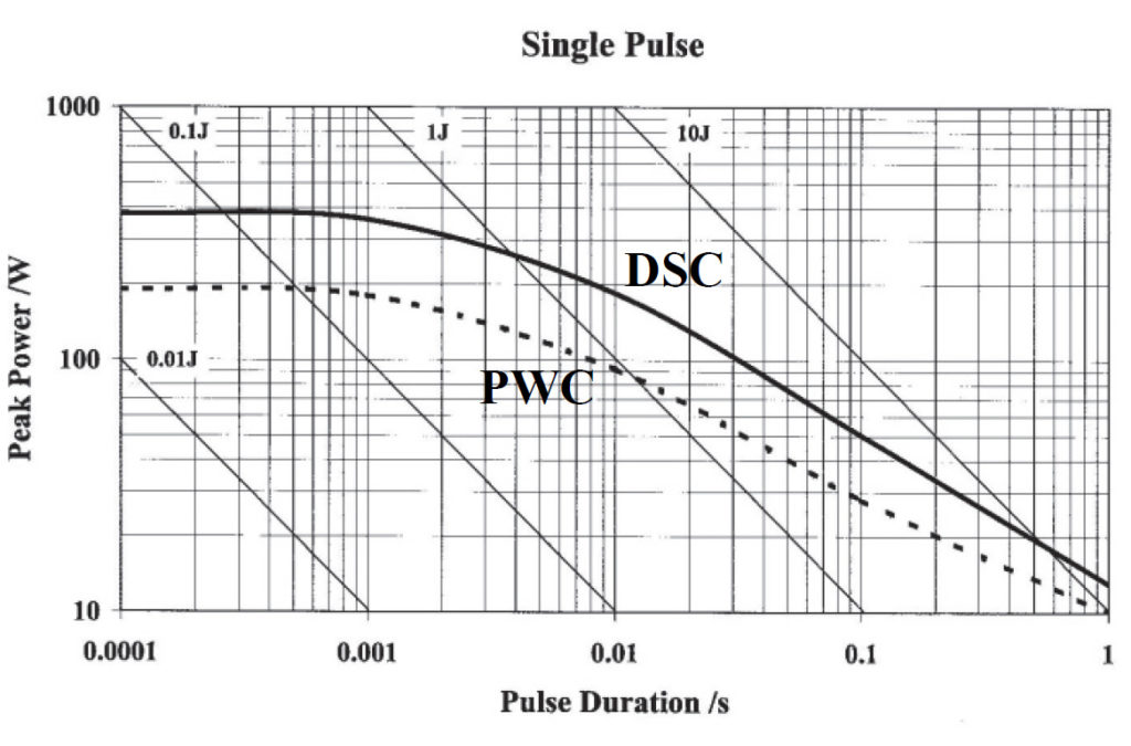
Figure 12 shows the performance achieved by both PWC and DSC in the 2512 chip size.
Earlier in 2019, the untrimmed single sided HPWC was joined by an untrimmed double sided chip, TT Electronics’ HDSC series. Omitting the trimming in these products removes the levelling off of peak power at durations below 10ms, increasing the peak power limit by 100% at 1ms, and by more for shorter durations.
Driver 3: Improving Stability and Reliability
Thin Film Technologies
Today, the vast majority of thin-film chip resistors use a sputtered thin film of nichrome (NiCr) for the resistive element. This technology was developed by TT Electronics IRC back in the 1950s and is used widely today. A second method was developed by Bell Labs in the 1960s. This uses tantalum nitride (TaN) with the big advantage that it is not at all susceptible to moisture, making it the technology of choice for very high reliability applications.
NiCr films suffer from the inherent weakness that they break down within seconds when moisture is in contact with the film and a voltage is applied. TaN survives that combination because it produces a stable, protective oxide layer; it is self-passivating. The material in this layer is tantalum pentoxide, which serves as the dielectric in tantalum capacitors, and renders tantalum virtually impervious to chemical corrosion. This is similar to the more familiar behaviour of aluminium, which forms a thin, mechanically stable oxide preventing progressive oxidation like the rusting seen in iron. However, because of the relatively high cost of the conventional TaN process, it has until now only been deployed in high reliability applications, such as in military and aerospace, high-end computer servers and some critical medical products.
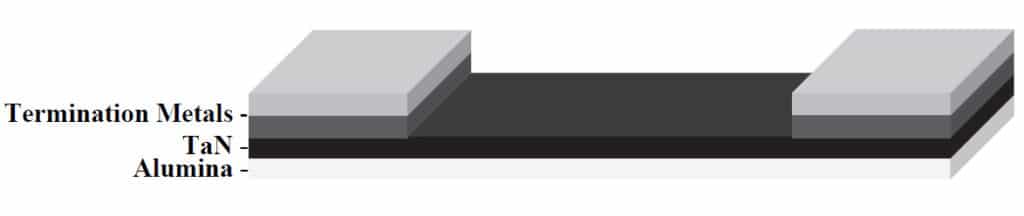
The internal structure of a TaN resistor is shown in figures 13 and 14. These show respectively the typical thin film structure after deposition by sputtering, and after the process of oxide growth. A printed epoxy layer (not shown) is normally added over the resistor element, and this gives mechanical protection and insulation, but importantly is not relied upon for moisture resistance.


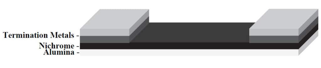
NiCr, by contrast, is totally dependent on the way it is protected against the environment. The basic way is to print a layer of epoxy on the top. But this material is not a hundred per cent impervious to water and there can be ingress under the edges. To increase the protection therefore, some manufacturers deposit a thin film of alumina (Al2O3) ceramic over the NiCr, below the epoxy layer. This helps but it is still not totally reliable; if the layer is scratched or otherwise damaged, water can still get in. With TaN, if something disturbs the oxidised layer, it will simply regrow; it is self-healing.
The internal structure of NiCr resistors is shown in figure 15 and that of the alumina passivated version in figure 16. A printed epoxy layer is added over the resistor element, and this is essential for the moisture resistance of the component.


Manufacturing Process
The main reason TaN has proven too expensive for many applications is that it uses a photo-lithography manufacturing process. A film is deposited on the substrate and is then coated with a photo-sensitive chemical. A mask is then placed on top of that leaving areas that are exposed to ultra-violet light. These areas can then be stripped away. This is a time consuming and costly process.
TT Electronics’ WIN series of TaN thin-film resistors changes that process to one using laser patterning. This is a far simpler process with the added large advantage that the deposition or front-end process can be done in advance creating a small number of standard substrates. Each block covers a broad range of finished values. When an order is received, the back-end process can be carried out to complete the order. This reduces lead times compared with photo-lithography where the whole the process has to be done from scratch every time an order is received.
Using laser scribing with automatic snapping equipment has achieved further cost and time savings compared with the diamond wheel dicing method used previously. Other manual processes have been replaced with automated equipment with improved process controls, sensors and computer monitoring. These have increased yields and reduced restarts.
The use of precious metals has been eliminated apart from in a small, targeted area where it improves the termination integrity.
Many engineers will be more familiar with tantalum in the field of capacitors. Here, the material has been known for unstable supply problems, leading at times to shortages and sharp price variations. However, TaN resistors use so little tantalum that this is simply not an issue. A typical tantalum capacitor has tens of milligrams of tantalum. A TaN chip resistor, on the other hand, has just a few micrograms, in other words a 10,000:1 ratio. Sensitivity to variations in tantalum price levels is therefore correspondingly negligible.
Currently, NiCr retains some technical advantages in terms of offering higher sheet resistances and therefore supporting higher ohmic values within a given geometry. It is also available in higher grades of precision, with TaN currently restricted typically to ±0.05% tolerance and ±10ppm/K TCR. However, thanks to its reliability benefits, TaN looks set to continue its expansion into commercial and industrial applications.
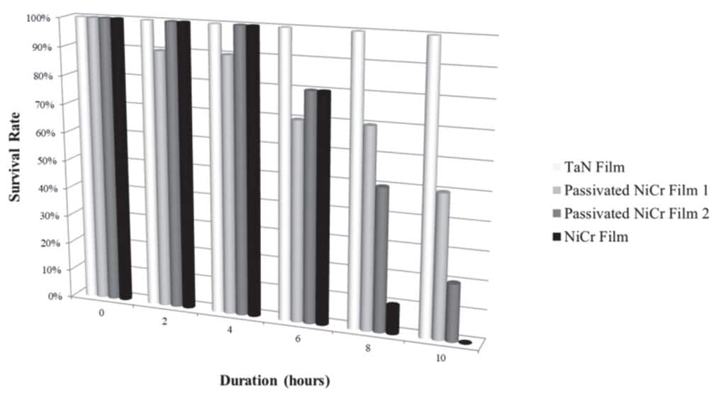
Benchmark Testing
In order to test the comparative moisture resistance of TaN film against NiCr and its passivated variant, a pressure cooker test was used. This highly accelerated life test method exposes components to saturated water vapour at a high pressure of 15psi at 120°C. The results, shown in figure 17, indicate that commodity NiCr types all fail after 10 hours of exposure. The addition of alumina passivation gives a measureable benefit, with 20 to 50% of passivated NiCr parts still operational after 10 hours. But only TaN film delivers a 100% survival rate under these challenging conditions, demonstrating a clear advantage over passivated NiCr resistors.

Conclusion
Film resistor technology has, by the standards of the wider electronics industry, a long life cycle. From origins in the 1930s it is still evolving to meet 21st century challenges. In particular it is adapting to meet the need for mitigating the environmental impact of short-lived electronic products. Furthermore, it is still pushing back the limits of safe operating area to meet the needs of high voltage or surge tolerant compact designs. And finally, reengineering of high reliability thin films is enabling their expansion into new market areas.
References
- “Perovskite Ruthenate-Based Lead-Free Thick Film Resistors” European Microelectronics & Packaging Symposium, M Prudenziate, B Morten, S Rane 18th June 2004
- “High-Power Thick-Film Resistor Designs Boost Power Density” ED Online ID #7494 8 November 1999
- “A model for line capacity design for PWB assembly systems” Zhongsheng Hua, Prashant Banerjee Robotics and Computer Integrated Manufacturing 19 April 2000
more 2nd PCNS symposium technical papers can be viewed and downloaded in pdf from EPCI Academy e-Proceedings: