by Marcel Manofu (1), Radu Voina (2), Cătălin Negrea (1)
(1) Continental Automotive Romania
(2) Technical University of Cluj-Napoca
OUTSTANDING AWARD PAPER BY PCNS ATTENDEES
presented by M.Manofu at the 2nd PCNS 10-13th September 2019, Bucharest, Romania as paper 2.2.
Abstract
Miniaturization leads to decreased supply voltages, which combined with higher current consumption of the integrated circuits (ICs) creates the need for more demanding power distribution network (PDN) requirements. The essential components in the PDN design are the decoupling capacitors. This paper presents an overview of multi-layer ceramic capacitors (MLCCs) characteristics that are of interest when used in power integrity (PI) analysis of automotive electronic systems. Design guidelines for decoupling capacitors selection and mounting board patterns are discussed by analyzing different types of capacitors and their parameter variations with DC voltage bias and temperature.
Introduction
The continuous increase in system complexity and operational frequencies of modern high-speed printed circuit boards (PCBs) creates new challenges in PDN designs by demanding higher current at lower voltages. This is due to the need of smaller packages to cope with the ever-decreasing available routing area. A typical PDN system, as seen in Figure 1, includes a voltage regulator module (VRM), bulk capacitors, PCB planes and interconnects, high-speed decoupling capacitors, and the package parasitics with the on-die capacitance of the load circuit.


The
goal of PDN design is to ensure that the system is able to transfer power from
the voltage regulator module (VRM) to the load circuit when it is needed and at
the requested rate, while minimizing noise generation.
An important step in achieving that goal represents the selection of decoupling
capacitors. The parasitic resistance and inductance associated with a mounted
capacitor, referred to as total equivalent series resistance (ESR) and total equivalent
series inductance (ESL) play an important role in overall PDN performance and
must be carefully evaluated.
If not analyzed properly, PDN elements can interact in undesired ways and lead to anti-resonances causing peaks in the overall PDN impedance. This can result in increased noise voltage at the load and can also negatively impact the stability of the VRM. The primary figures of merit when analyzing power integrity are noise voltage, power rail impedance, effective loop inductance. [1]
Influencing factors on capacitance
Capacitors are among the most critical components needed for any electronic design and essential for determining the system’s stability and reliability. The increasing demand for high charge density is met by using high dielectric constant materials and small thicknesses of the dielectric layers. The most common capacitors are the MLCCs, which are produced from alternating layers of metal and ceramic. Since they are non-polarized devices, they are best suited for use in high frequency decoupling applications.


Capacitor ESL determines the series resonant frequency (SRF) of the capacitor as it forms a series resonance with the capacitance. The ESR determines the minimum impedance reached at the resonant frequency, having direct impact in the total number of capacitors required to achieve certain target impedance at a particular frequency.
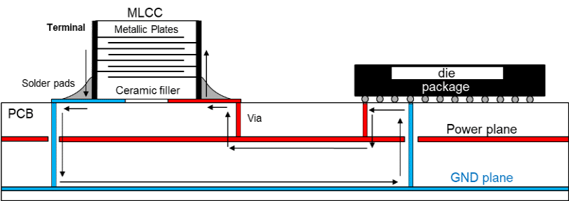
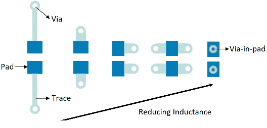
Total ESL is influenced by three elements: capacitor height, pad layout and power plane spreading inductance. These elements describe the loop that current must flow in, the bigger the loop, the higher the inductance. The biggest contribution to the inductance is made by the mounting pad structure. Minimizing the length of the vias that connect capacitor pads to the power and ground planes, as well as keeping those vias close to each other, as shown in figure 3, helps in minimizing the ESL. [5]
Decoupling capacitor location has significant impact on power plane loop inductance which directly affects the PDN frequency response. Placing capacitor further away from load circuit power pins, thus increasing the loop inductance, can lead to ground bounce noise and coupling from power planes to high-speed signal traces. Capacitor placement should be done in such way as to minimize the current path of the inductive loop. [4]
As voltage variation is dependent on inductance, low ESL capacitor types are increasingly replacing conventional ceramic capacitors. The main advantage is reducing the overall occupied space and cost of the decoupling solution by requiring fewer capacitors for similar PDN performance obtained with standard MLCCs.
The inductance of any device is determined by its length to width ratio, known as the aspect ratio.
As MLCCs are long and narrow, the natural evolution was to make them short and wide, thus reverse geometry capacitors were designed, which provide up to 50% lower inductance for a few fractions increase in cost over traditional MLCC. [3] Three terminal type capacitors offer even lower ESL by using an internal parallel reference electrode structure, nonetheless it costs several times more than a traditional MLCC and is therefore avoided in cost sensitive automotive PDN designs. [7]

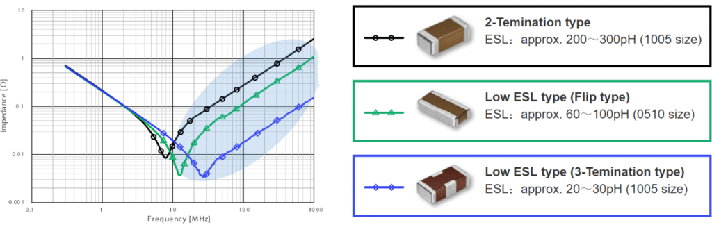
Figure 4 highlights the dominant inductive impact on the frequency response of different termination types for ceramic capacitors of the same datasheet capacitance rating.
The
continuous downsizing and use of higher dielectric constant materials for Class
II capacitors, used heavily in automotive PDN designs, has resulted in
degrading capacitance stability at various operating conditions. [8]
Very thin layers of Class II ceramics lead to a greater dependability of the
actual capacitance on the DC and AC voltage biases, and can also show a
stronger temperature dependence that stated in datasheets. It was also shown
that bias sensitivity of X7R parts is not necessarily better than that of X5R,
sometimes not even from the same vendor. [2]
All major vendors supply at least DC bias information with their MLCC parts, nonetheless there is an additional challenge for the user which has to fold the bias-dependent vendor data into a model that can be used in the simulation tools.
Capacitor models
Simple capacitor models were preferred in the past when simulating large circuits in order to minimize simulation run time. These minimal models use only the nominal capacitance of the device, minimum ESR over a broad frequency range and the lowest inductance measured. The first problem that arises is that ESR and ESL are a function of frequency and may vary significantly from the minimum value given in the RLC model resulting in inaccurate impedance simulation mainly at frequencies above self-resonance. Figure 5 Typical model used for MLCC [9]


In Figure 5 a typical MLCC model provided by manufacturers is presented. Compared to the simple model it includes also a parallel resistive element to account for the leakage or insulation resistance and may include a parallel RC circuit to account for the dielectric absorption behavior. For high capacitance components, above 10uF, series RL networks can be added to account for the change in inductance at higher frequencies. [9]
Usually vendors provide also Touchstone models for their MLCCs, as they are easily handled by simulation tools and reduce simulation time compared to SPICE models.
Even though the model presented above comes very close at predicting the real capacitor behavior, it does not consider 2nd order parameters, like temperature and DC bias. These parameters have great importance when performing a corner-case analysis, procedure which is mandatory in the design of safety-critical electronic devices, as it is the case for automotive electronics.
The demand for component models that dynamically reflect dependence on the circuit operating conditions is continuously increasing. As an answer to this need vendors started offering the so-called dynamic models, which allow for realistic assessment of the PDN performance under worst case conditions.
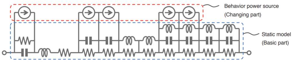
In Figure 6 it is presented an example of such a dynamic model for a MLCC. In-circuit DC bias is considered through the use of several voltage controlled current sources, while the temperature bias can be added manually as an input parameter to the SPICE model.

As more vendors start to offer these models for their components and as they are becoming more accurate through new calculation functions, all EDA circuit simulator vendors will have to offer full support for dynamic models libraries, which become a must when accurate circuit simulations are needed.
Power Distribution Network Performance
PDN performance evaluation was not considered a major criterion in early PCB designs. In today’s electronic modules with lower voltage, higher current and smaller voltage noise margin, PDN performance becomes important and should be evaluated in early stages of the PCB design process.

To
assess the performance of a PDN, one must first perform a static analysis in
which the DC current capability of the power rail is evaluated. This is
determined by the geometry of the net and the material conductivity.
This step is referred to as IR drop analysis and its goal is to ensure that for
the specified DC current demand, the voltage drop across the PDN will not cause
the voltage level at the load to exceed the operating limits.
To obtain small IR drop it is recommended to use short and wide power net traces. Large number of discontinuities caused by clearance holes of passing signal vias result in the so-called “swiss cheese effect”, which increases the IR drop and also the plane spreading inductance. Insufficient via interconnect current carrying ability can be another cause of IR voltage drop increase, effect known as via starvation.
Once the IR drop is minimized to an acceptable level, the designer proceeds with the dynamic PDN evaluation, referred to as AC impedance analysis. The objective of this analysis consists in ensuring that the PDN impedance value seen from the pins of the load device is below a certain target impedance.
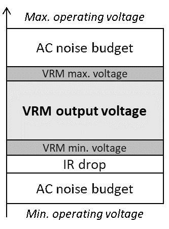
The target impedance, named , relates the maximum allowed voltage fluctuation, referred to as AC noise budget, to the dynamic current required by the load device. In Figure 7 it is shown how this noise budget is obtained considering the VRM output specifications, the IR drop value and the load circuit operating range. Having also the maximum dynamic current step of the load circuit, the target impedance can be determined as: .
A good PDN design is considered when the impedance profile is well below the target impedance. A typical frequency response of a PDN is shown in Figure 8 with highlight on the anti-resonances and their main contributors.


The elements constituting the PDN add significant parasitics which can lead to anti-resonance peaks in the impedance profile and violate the target impedance. A flat PDN impedance at lower frequencies is desired as it helps also in reducing the package anti-resonance at higher frequencies. When the PDN is not designed appropriately, power supply voltage fluctuation can occur and interfere with IC operation, degrade signal integrity and increase noise emission.
Evaluating these effects is done using specialized electromagnetic (EM) simulation tools which allow the extraction of PCB parasitics in the form of Touchstone models, which can be used together with the VRM model, load circuit package and die capacitance and capacitor models to form a simulation schematic of the entire PDN system. To note that capacitors are effective at lowering the impedance but up to a point where their impact will not be visible anymore due to the spreading inductance becoming dominant.
PDN simulation using dynamic capacitor models
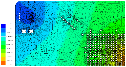
To evaluate capacitor modeling impact on PDN performance a test layout was realized. A 10-layer stack-up was chosen with the power net routed on layers 5 and 6, while the ground net on layers 4 and 7. Figure 9 highlights the power plane routing, location of the VRM, capacitors and the load IC, which is a processor with two internal Dual ARM logic cores.


The processor datasheet specifies an operating voltage range between 1.35V and 1.5V. The VRM module is configured to have an output voltage of 1.425V, while considering also the set-point accuracy and switching ripple will result in a minimum guaranteed supplied voltage of 1.4V.

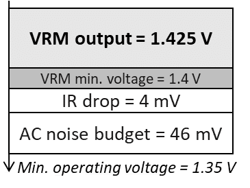
For the IR drop analysis a worst-case current consumption of 3.2A was considered and results in Figure 10 show a voltage drop across the PDN of 4mV. The IC presents separate internal rails for each of the Dual ARM core, for simplicity we will analyze the impedance of only one rail, whose power pins are highlighted in Figure 9. Calculating the remaining AC voltage noise budget as shown in Figure 11 and knowing the maximum dynamic current step of an ARM core that is 1A, a target impedance of 46mΩ is obtained.
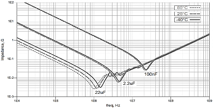
Decoupling solution evaluation was done by using a library with dynamic SPICE models provided by a vendor. To better observe the external bias impact on PDN impedance, we chose capacitors with 20% tolerance. Figure 12 shows the impedance variation with temperature of usual MLCCs used in automotive PDN design. As shown in Figure 13, DC voltage bias impact is significant if we get close to the capacitor’s rated voltage, and as our circuit operating voltage is only 1.5V the impact on SRF shift will be minimal.


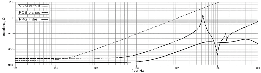
The frequency responses of individual PDN components except the capacitors are presented in Figure 14 below.

Putting together all the PDN components including the bulk and high-speed decoupling capacitors will result in the impedance profile seen from the load IC pins shown in Figure 15. A DC bias voltage of 1.5V was applied to the circuit through the VRM model and three temperature scenarios were simulated: -40, 25 and 85 °C. To evaluate a realistic temperature bias environment, copper conductivity was modified in the EM simulation tool according to the temperature in each simulation scenario.


Results show that capacitance change of MLCCs in the presence of DC voltage and especially temperature bias have a significant impact on the overall PDN impedance profile. It was found that this effect is more significant in larger capacitance value components. The shift in SRF value of the bulk capacitance combined with the decrease in total ESR at lower temperatures favors a higher value of the first anti-resonance peak affecting the “flatness” of the impedance profile.
Conclusions
The mounting pad structure and board location of MLCCs are important in determining the total ESL and ESR and play a major role in determining overall PDN performance. In addition, MLCCs’ frequency characteristics can be significantly degraded by DC voltage bias and temperature bias and must be carefully evaluated.
Corner-case analysis of today’s automotive electronics requires the use of component models that dynamically reflect dependence on the circuit operating conditions, therefore it is very important for vendors to accurately describe their components and provide dynamic models to be used in simulation tools.
References
- Steve Sandler, “Power Electronics vs. Power Integrity”, PICOTEST.com, January 2019
- Tanmoy Roy, Larry Smith, “ESR and ESL of Ceramic Capacitor Applied to Decoupling Applications”
- John D. Prymak, “Designing and Measuring Low ESL in Capacitors”, DesignCon East 2005
- Shirin Farrahi, Ethan Koether, Mehdi Mechaik, Istvan Novak, “Effect of Power Plane Inductance on Power Delivery Networks”, DesignCon 2019
- https://www.speedingedge.com/PDF-Files/X2Y%20vs%200402%20081605.pdf
- https://product.tdk.com/info/en/products/capacitor/ceramic/mlcc/technote/solution/mlcc07/index.html
- https://passive-components.eu/high-cv-mlcc-dc-bias-and-ageing-capacitance-loss-explained/
- Istvan Novak, “DC and AC Bias Dependence of Capacitors Including Temperature Dependence”, DesignCon East 2011
- John D. Prymak, Peter Blais, William Buchanan, Edward Chen, Ken Lai, Gianpietro Malagoli, Allen Mayar, Matti Niskala, Axel Schmidt, Paul Staubli, Boris Vildaver “Capacitor EDA Models with Compensations for Frequency, Temperature, and DC bias”, CARTS Conference 2010
- https://www.murata.com/~/media/webrenewal/about/newsroom/tech/capacitor/mlcc/ta1681
more 2nd PCNS symposium technical papers can be viewed and downloaded in pdf from EPCI Academy e-Proceedings: