


The paper presents effects of derating on performance and reliability of Solid Electrolytic and Polymer Tantalum capacitors manufactured with conventional technology and flawless dielectric technology (F-Tech) combined with simulated breakdown screening (SBDS). Solid tantalum capacitors that can be used in high-reliability applications with low/no derating and are efficient, reliable, and cost effective are under discussion.
The paper was prepared by Yuri Freeman and Phil Lessner, KEMET Electronics, YAGEO Group at the 4th PCNS 10-14th September 2023, Sønderborg, Denmark as paper No. 3.5.
Capacitor derating, reducing application voltage Va vs. rated voltage Vr decreases electrical field in the dielectric F = Va/d, where d is the thickness of the dielectric, and therefore reduces failure rate and improves capacitor reliability. Derating is traditionally used at elevated temperatures like Va ≈ 0.67Vr at T = 125oC while Va = Vr at T ≤ 85oC in surface mount (chip) Solid Electrolytic Tantalum (Ta) capacitors with manganese dioxide cathode [1].
Derating 50% at normal temperatures was recommended to chip Solid Electrolytic Ta capacitors based on the hypothesis about ignition failure mode in these capacitors [2]. According to this hypothesis, at breakdown event with rapid temperature increase, oxygen released from MnO2 cathode at its transformation into low manganese oxides ignites Ta anode sintered in vacuum with fine Ta powder. The heat released at burning of the Ta anode in failed Solid Electrolytic Ta capacitor causes massive damage to the surrounding circuit board, while 50% derating reduces probability of failure preventing this massive damage.
During halve-a-century of their applications, there were no reports of the ignition failures in chip Solid Electrolytic Ta capacitors at normal application conditions.
Recent investigation showed that black marks on the surface of the failed Solid Electrolytic Ta capacitors were the result of the carbonizing of the external mold compound under the heat propagated from the breakdown channel in the dielectric [3]. Moreover, some of the failed chip Polymer Ta capacitors also have black marks on their surface. Nevertheless, 50% derating became the rule for applications of Solid Electrolytic Ta capacitors.
The serious drawback of the 50% derating of Ta capacitors is 10x or more increase in size of the capacitor and thus drastic loss in volumetric efficiency CV/cc, which is most important advantage of Ta capacitors in comparison to all other major types of the capacitors.
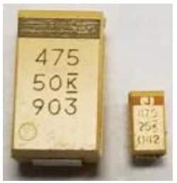
As an example, Fig. 1 shows A-case 4.7 uF – 25 V Ta capacitor and D-case 4.7 uF – 50 V Ta capacitor that should be used in 25 V application with 50% derating.
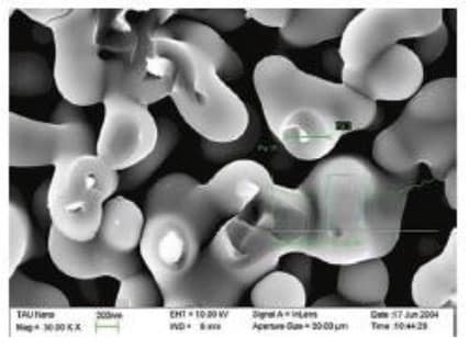
The large increase in size of Ta capacitors with 50% derating is caused by the combination of increased thickness of the dielectric in higher voltage Ta capacitors and decreased surface area of Ta anodes due to coarser Ta powder in these anodes. As an example, Fig. 2 shows the breakage of the formed Ta anode with white areas representing Ta and grey areas representing Ta2O5 dielectric.
As one can see from Fig. 2, the oxide dielectric consumes Ta from the Ta particles leaving small necks between the particles. Growing thicker dielectric on this anode will consume all Ta from the necks disrupting conductivity of Ta anode and causing total loss of capacitance. Only coarser Ta powder sintered at higher temperature provides sufficiently large necks and open pores to grow thicker dielectric.


Besides the sharp increase in size, weight and thus cost of Ta anodes, 50% derating of higher voltage Ta capacitors causes loss (not gain) in the reliability.
Fig. 3 shows breakdown voltage (BDV) dependence on the formation voltage in Solid Electrolytic Ta capacitors. Formation voltage (Vf) determines the thickness of the Ta2O5 dielectric as Vf = a*d, where constant a ≈ 2 nm/V at 80oC formation.

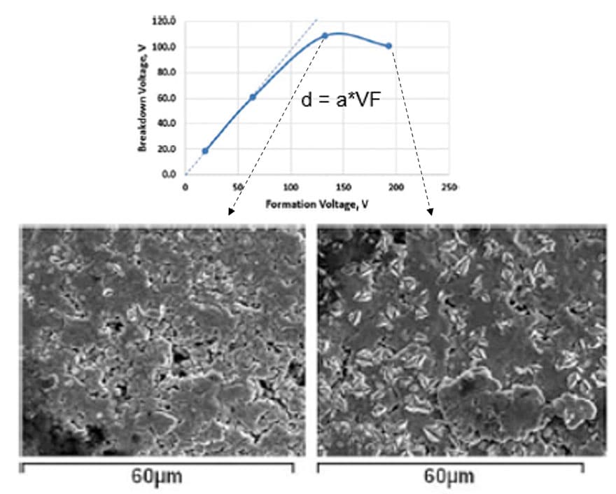
Fig. 4. (below) SEM images of Ta anodes formed at formation voltages 130 V (left) and 190 V (right).
As one can see from Fig. 3, BDV reaches maximum at about Vf = 150 V and then decreases with increasing formation voltage. Fig. 4 shows scanning electron microscopy (SEM) images of the dielectric on Ta anodes formed at 130 V before reaching maximum point and 190 V after reaching maximum point in BDV.
According to Fig. 4, there are characteristic defects, cracks, in the dielectric with 190 V formation. The size and number of these defects is much lower at 130 V formation. The nature of these defects relates to amorphous structure of the Ta2O5 film, which demonstrates good dielectric properties, but is thermodynamically unstable [3]. Small crystalline inclusions with higher density than amorphous phase grow in amorphous matrix of the dielectric generating mechanical stress and eventually cracking in the dielectric. The crystallization process accelerates with increasing thickness of the Ta2O5 dielectric. This is major reason that maximum working voltage in Ta capacitors is much lower than working voltages in ceramic, film, and aluminum electrolytic capacitors.
To suppress growth of the crystalline inclusions in amorphous matrix of the dielectric, flawless dielectric technology (F-Tech) was developed [3]. The F-Tech includes numerous process steps during the anode manufacturing that eliminate local contaminations with carbon, oxygen, and other impurities that function as the seeds for the crystalline inclusions. F-Tech also uses special formation conditions to suppress the crystallization process, including formation in electrolytes containing organic solvents [4,5].
The important part of the F-Tech is optimal ratio between the formation voltage Vf and rated voltage Vr. Traditionally higher Vf/Vr design and thus thicker dielectric is used in high reliability products in comparison to Vf/Vr in commercial products. At the same time, high Vf can provoke crystallization of the amorphous Ta2O5 dielectric in higher voltage Ta capacitors even manufactured with F-Tech. The long experience of development, manufacturing and field application of Ta capacitors showed that these capacitors are highly reliable when BDV in finished parts is equal or exceeds double rated voltage [3]. Fig. 5 shows cross-sections and SEM images of formed Ta anodes in X-case Solid Electrolytic Ta capacitors 6.8 uF – 50 V manufactured with F-Tech and traditional for high reliability design Vf/Vr ≈ 5 and optima design Vf/Vr ≈ 3. Finer powder in Ta anodes was used with optimal design in comparison to that with traditional design.
As one can see in Fig. 5, the capacitors with optimal design have smaller size Ta anode and dielectric in these capacitors is practically defect free while there are cracks in the dielectric of the capacitors manufactured with traditional design. And BDV in finished Ta capacitors is higher with optimal design in comparison to BDV with traditional design.


Even with most advanced technology, there is a probability that some Ta capacitors have small defects in the dielectric that will grow during field application and cause failure. While these defects are small, they are not detectable by testing dc leakage. At the same time, even small hidden defects in the dielectric reduce BDV in finished capacitor.
Since BDV test destroys all the capacitors, simulated breakdown screening (SBDS) was developed that allows screening parts with low BDV without affecting population of the capacitors [6,7].
The SBDS includes actual BDV testing of a sample from every production batch to determine parameters of screening and is performed at the end-of-line on all Ta capacitors manufactured with F-Tech
Comparison of the failure rate in Solid Electrolytic Ta capacitors manufactured with conventional technology and F-Tech/SBDS was performed by the capacitors user in high reliability applications [8].
For the same capacitance and voltage, the failure rate was 1.65E-3 – 2.6E-3 in “Industry Average” capacitors with conventional technology and 3.6E-11 in capacitors manufactured with F-Tech/SBDS.
Besides much lower failure rate, F-Tech and SBDS also provide much steeper reduction in the failure rate with derating in comparison to traditional technology (Fig. 6).

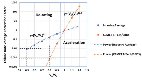
According to Fig. 6, 10% derating of Solid Electrolytic Ta capacitors manufactured with F-Tech/SBDS provides the same reduction in the failure rate as 40% derating of the capacitors manufactured with traditional technology
The major advantage of Polymer Ta capacitors in comparison to Solid Electrolytic Ta capacitors is their lower equivalent series resistance (ESR) coming from higher conductivity of the inherently conductive polymer cathode in comparison to the manganese dioxide cathode. In recent years Polymer Ta capacitors achieved significant improvements in their performance and reliability and F-Tech/SBDS made important contributions to these improvements [9].
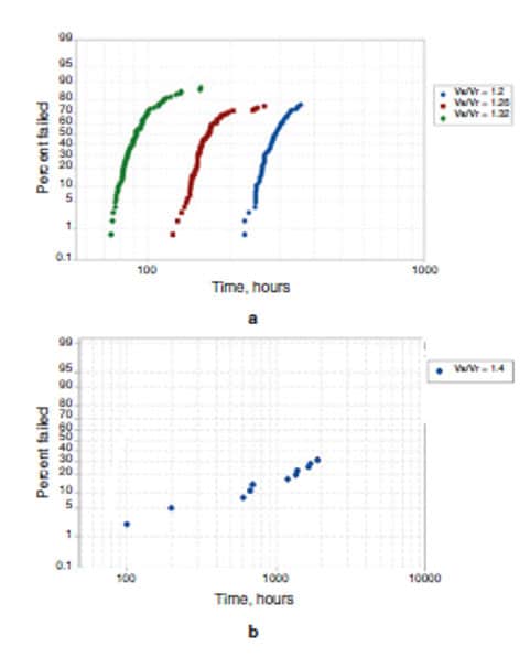
Particularly, F-Tech and SBDS changed wear-out failure mode in Polymer Ta capacitors manufactured with traditional technology to now wear-out and reducing with time failure rate. Fig. 7 presents cumulative percent of failed parts versus time in surface mount H-case Polymer Tantalum capacitors 220 uF – 25 V manufactured with conventional technology and F-Tech/SBDS and tested at 105oC with different acceleration factors Va/Vr.
As one can see in Fig. 7a, Polymer Ta capacitors manufactured with conventional technology demonstrate wear-out behavior with no failures at the initial stage of the accelerated testing following by the failures of the majority of the parts within short time interval.
The time to wear-out decreases sharply with increasing Va/Vr. In contrast to that, Polymer Ta capacitors manufactured with F-Tech/SBDS (Fig. 7b) have no wear-out even at higher Va/Vr.
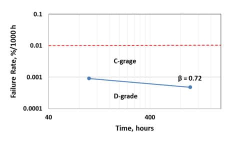
Based on the data presented on the Fig. 7b, the failure rate was calculated for the Polymer Ta capacitors manufactured with F-Tech/SBDS using Weibull equation for the voltage acceleration factor and Arrhenius equation for the temperature acceleration above 85oC (Fig. 8).

According to Fig. 8, Polymer Ta capacitors manufactured with F-Tech/SBDS have the lowest D-grade failure rate and it decreases with time like the failure rate in Solid Electrolytic Ta capacitors.


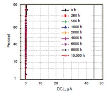
Polymer Hermetic Seal (PHS) Ta capacitors were developed to substitute Wet Ta capacitors with liquid electrolyte cathode having high ESR especially at higher frequency and lower temperature. Currently PHS Ta capacitors are the most advanced Ta capacitors combining low ESR inherent to all Polymer Ta capacitors with high working voltages and low and stable dc leakage. As an example, Fig. 9 presents DCL distribution in B-case 100 uF – 60 V PHS Ta capacitors during 10,000 h life test at 85oC and rated voltage (no derating).
All PHS Ta capacitors are manufactured with F-Tech/SBDS [10]. Controlled amount of humidity is added to the hermetic packaging [11] that eliminates anomalous charge current (ACC) and leakage current degradation observed in non-hermetic chip Polymer Ta capacitors in dry environment.
Additional advantage of PHS Ta capacitors is their record high volumetric efficiency CV/cc. As an example, B-case 550 uF – 35 V PHS Ta capacitors have 11.7 times higher capacitance than X-case 47 uF – 35 V chip Polymer Ta capacitors. At the same time the ratio in volume between these capacitors is equal to 3.6, which gives 3.3 times higher CV/cc in PHS Ta capacitor in comparison to non- hermetic chip Polymer Ta capacitor. Besides, solder plated metal package can provide some protection from the radiation that damages polymer chains and thus increases ESR in non-hermetic Polymer Ta capacitors [12]
Conclusion
In conclusion, derating 40%-50% at normal temperatures of Solid Electrolytic and Polymer Ta capacitors manufactured with conventional technology results in sharp increase in the size, weight, and cost of the capacitors.
This derating also reduces reliability of the higher voltage Ta capacitors due to acceleration of the crystallization process in the amorphous matrix of the dielectric.
At the same time Solid Electrolytic and Polymer Ta capacitors manufactured with F-Tech and SBDS are efficient, reliable, and cost effective and can be used with low/no derating in mission critical applications.
The optimal choice between Solid Electrolytic and Polymer Ta capacitors and non-hermetic chip and hermetic packaging depends on the specific application conditions such as temperature, humidity, and radiation.
Polymer Hermetic Seal (PHS) Ta capacitors combine low ESR inherent to all Ta capacitors with polymer cathode with record high working voltages, record low and stable dc leakage, and record high volumetric efficiency.
References
- MIL-PRF-55365H, 2013
- J. Prymak, 21st Capacitor and Resistor Technology Symposium (CARTS), St. Petersburg, FL, 2001, p.25
- Y. Freeman, Tantalum and Niobium-based Capacitors: Science, Technology, and Applications, 2nd edition, Springer, 2022
- B.J. Melody, J.T. Kinard, D.A. Wheeler, US Patent 5,716,511
- J.T. Kinard, B.J. Melody, D.A. Wheeler, US Patent 6,480,371 B1
- Y. Freeman, US Patent 7,761,603 B2
- J. Paulsen, E. Reed, Y. Freeman, US Patent 8,441,265 B2
- W. Winkel, E. Rich, 34th Capacitor and Resistor Technology Symposium (CARTS), Santa Clara, CA, 2014, p.175
- Y. Freeman, P. Lessner, Appl. Sci., 11 (12), 5514, Special Issue Multifunctional Polymers and Composites, 2021
- DLA 13030, 2015
- J. Chen, Y. Freeman, S. Hussey, US Patent 8,379,371 B2
- A.K. Anbalagan et al., RSC Advances 11 (34), 2021, p. 20752