

In this paper SERMA TECHNOLOGIES presents failure statistics of connectors from field return analyzed during the last 10 years. The article analyze main defects encountered during failure analysis and associated mechanisms / root causes (if identified).

This paper was presented by Cédric Favarel, Serma Technologies, Pessac, France at the 4th PCNS 10-14th September 2023, Sønderborg, Denmark as paper No.1.2.
INTRODUCTION
With more than 20 years of experience from the field and thousands of analyzes carried out, we now have unique know-how on all types of electronic components, boards and systems.
On one hand, the realization of DPA (Destructive Physical Analysis) or CA (construction analysis) allows the analysis of the quality of the products in relation to MIL or ESA/ESCC standards or in relation to the “state of the art”. All these analyzes are carried out using non-destructive testing such as visual inspection, radiography or acoustic microscopy and destructive testing such as microsection, shear tests, tensile tests, solderability, etc.
On the other hand, failure analyzes make it possible to determine the modes and mechanisms of failure in order to understand and act according to the problems encountered by the actors of industrial development of today, whatever their field of activity. Then carry out electrical and physical analyzes on the components. Many means of sample preparation, observation and analysis are at our disposal: electrical test, optical microscopy, acoustic microscopy, 2D and 3D X-ray radiography, infrared thermography, mechanical and chemical opening of package, micro-section, SEM (Scanning Electron Microscope) observations, material analysis by EDX, FTIR (Fourier-transform infrared spectroscopy), XPS (X-ray photoelectron spectrometry), SIMS (Secondary-ion mass spectrometry), TEM (Transmission Electron Microscopy) observation and fault localization.
This paper present failure statistics of connectors from field return analyzed during the last 10 years. Presentations of the main defects encountered during failure analysis and description of the associated mechanisms. Focus and description on the followings failures modes, causing failure (as open circuit / short circuit / high contact resistance or intermittent defect): package/insulation issue; poor electrical contact; press fit or soldering issue; pollution; metallic migration; fretting corrosion and wear out, tin whiskers.
In addition to all those material characterization facilities, we will focus on how the use of partial discharge can allow to locate insulation weakness issues on connectors comparatively to classical dielectric stress test.
Failure analysis statistics of our laboratory
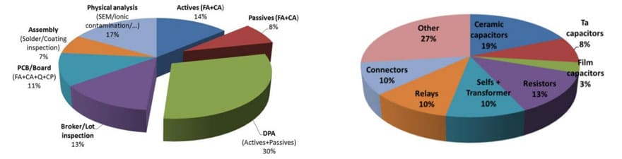
Since 10 years more than 20,000 analyzes were carried out, including nearly 2,000 in passive components (failure analyzes and construction analyses), of which 200 concern connectors. The statistics are shown in Fig. 1:

MAIN DEFECTS ON CONNECTORS FROM FIELD RETURN
1-Package Defect
The main defects observable on package are related to delamination or cracks generating a path, and then the possibility of humidity, contamination to make species migration under polarized conditions, that lead to leakage path, up to short circuit between leads. Crack or delamination may come from initial parts weakness, or too severe assembly conditions (humidity management/ reflow profile/handling,…)
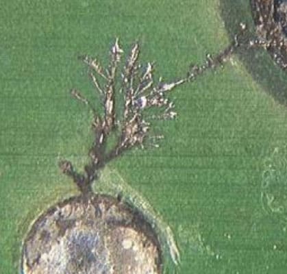
2-Wear-Out and Fretting Corrosion
Fretting wear is generated by small-amplitude movement leading to the formation of small debris particles at a mechanical interface. In electronic connectors, the amplitude of this micromotion ranges from a few µm to about 100µm. Micromotion is caused by external vibrations and/or changing temperature due to differences in thermal expansion coefficients of the mating materials.

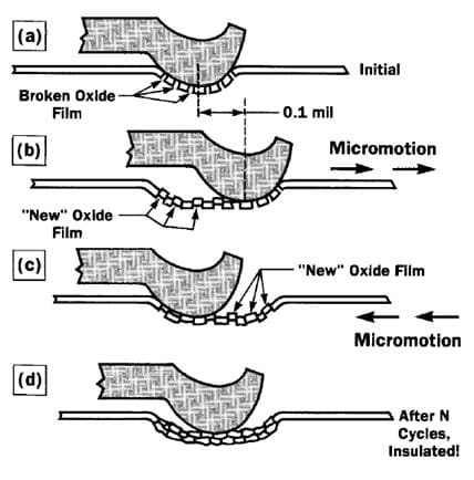
Fig. 2: Fretting corrosion mechanism
Wear out is observed when wear particles are generated (gold, nickel and copper) without oxidation. During analysis by EDX, nickel and copper could be detected but without oxygen element. Since the prime plate is in place to protect the base metal (non-noble metal), wear is of prime concern in the design of a contact. If the prime plate is worn through, the exposed under-plate of substrate (which are non-noble systems) are susceptible to the corrosion process. The term wear indicates the forced removal contact material during the sliding action that occurs. This removal may be a result of the transfer phenomena (transfer of material from one contact surface to the other) or loss due to loose particles caused by the mating action. There are three wear mechanisms.
- Abrasive: wear resulting from rough, sharp hard materials or a combination thereof in contact with a softer material. An example of these surfaces are the lead-in chamber of a printed circuit board, screw machine products, blunt end mating pins, etc.
- Brittle fracture: this is the cracking of a plated surface perpendicular to the direction of sliding. This type of wear can occur on low strength materials or a poorly controlled plating process.
- Adhesive: this is the most common type of wear. It results from micro cold welding dependent to the force. The higher the normal force are, the more susceptible the surfaces are to this type of wear.
Fretting corrosion is due to oxidation of fretting debris. Oxygen is clearly detected by EDX. The phenomenon leads to increased electrical contact resistance leading to the risk of contact loss or intermittent. The details of the fretting corrosion mechanism is shown in Fig. 2.
In this phenomenon choice of coating are particularly important. Tin or tin alloy coatings are cost effective and reliable alternatives to gold if used according to some precautions. Mating tin contact to gold contact is not recommended. Also tin is not recommended at high temperature as sliding or wipping with this kind of contact. In comparison gold is an excellent electrical conductor and a highly stable noble metal which exhibits the following contact properties. It can be used in corrosive environments (when sufficiently thick), for high durability, high temperature and is less susceptible to fretting degradation. However gold coatings require the use of a suitable underlayer such as nickel to prevent copper diffusion into gold. Absence of an oxide layer allows low voltage connection with low normal force. Soft gold will wear off easily while hard gold offers more protection. Gold should be sufficiently thick for the application from flash gold (50-100nm) for use with single mate situations or low reliability, to thick layer (up to 1µm) for high reliability and high cycle situations.
If micromotions are important, underlayers of contacts can be altered, accelerating fretting-corrosion.
3-Pollution
Pollution make a direct insulative layer leading to an increase of the contact resistance. Pollution could mainly come from assembly process (special care should be taken when using varnish coating), or with external environment for example NaCl salts at the interface of contacts (conductive in water and insulating in its crystalline form).
4-Poor Electrical Contact

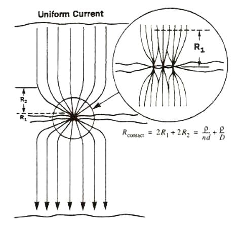
Actual electrical connection is made through small asperities. These asperities are locations where metal to metal contact is made across the contact interface and depending the type of coatings, material and mating force only 1% of the apparent contact area is actually making contact. In this configuration phenomenon of constriction resistance occurs, as shown on Fig. 3.
Actual current flow occurs through the small asperities where metal-to-metal contact takes place. Should these contact regions reduce in size due to oxidation, contamination, reduced normal force, etc. thus the resistance increase. Increasing resistance can cause local heating that can increase oxidation and further increase the resistance generating a thermal runaway. Eventually the resistance can increase to the point of contact failure.
Another mechanism could occur at contact interface: resistance film formation. Understanding nickel, copper and tin oxide formation is important to put in proper perspective when considering functional limitations of connectors. In presence of Cl2, H2S, NO2 or SO2, complex compounds can appear and then film resistance can growth over time and resistance increase. Depending the plating choice of the contact interface different resistance film formation can occur.
With gold plating, pore free gold will not react unless base metal porosity exists. If base metal porosity exists, the pore may become active (porosity is a result of discontinuities that expose the under-plate or base metal). An active pore is one which penetrates through the gold or gold/nickel to the base metal and allow corrosion products to exit and spread on the contact surface.
With gold flash/PdNi plating, if the gold flash is porous or worn out due to the number of mating cycles thus exposing PdNi to the environment, reactions will occur particularly when SO2 is present (mainly in industrial area).
With tin (alloy) plating, due to softness of tin if inappropriate normal forces are used, this material may react and create oxide. In most of case this is not an issue because oxides are easily displaced out of the contact area, unless if exposure occurs or thick layer of copper/tin intermetallic exist.
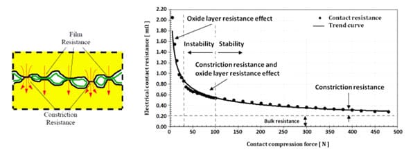
Contact normal force is a critical parameter to take in account during design process. Increasing normal force (according to requirements depending on the contact finishing) provides more contact points and decrease contact resistance. The curve Rcontact versus Fcontact will differ with each type of contact material. Low contact force leads to high current density per spot and then hot spot risk. On the contrary, higher force will lead to less current density per spot as shown on Fig. 4.

5-Press Fit Issue
Main risks in press fit assembly are due to cracks and/or deformation of PCB due to mismatch between pin diameter, via diameter and pressure. Deformation of the metallized via, top, bottom and internal copper layers should respect the specifications in terms of copper thickness after insertion of the lead in order to avoid crack and open circuit. Cracks in the PCB along glass fibers also should respect the minimum dielectric distance in order to avoid short circuit with nearby copper tracks.
6-Electrochemical Migration (ECM)

Electrochemical migration (ECM) is the dissolution and movement of metal ions in presence of electric potential (low voltage potential needed), which results in the growth of dendritic structures between anode and cathode and may significantly decrease the insulation between conductors until short circuit occurs. The main factor facilitating the ECM is humidity (only a water film needed as condensation or relative humidity) and the presence of pollution (low quantity needed usually coming mainly from flux). In the presence of water, ECM can go very quickly.
Usually the process involves several stages: water adsorption, anode metal dissolution, ion accumulation, ion migration to cathode, and dendritic growth, as shown in Fig. 5. The growth of the dendrite takes fraction of a second, during which time the resistance between anode and cathode drops almost to zero. This kind of failure mechanism could generate intermittent issue as the dendrite could growth, generate short circuit and then act as a fuse and the short circuit disappear instantly. If the conditions of dendrite growth are still present, the mechanism repeat itself.
7-Tin Whiskers
Sudden failures and intermittent problems sometimes occurs in electronic devices associated with tin whiskers because of their ability to short closely spaced electronic circuits.

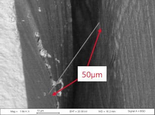
Whiskers were found to grow across circuit connections and, because of their thin, brittle nature, would break free and lodge across circuits.
The exact cause of tin whisker growth is still not fully understood. It seems that the energy for growth comes from microstrains present in the tin or from externally applied pressure.
Fig. 6, an example of whisker observed by SEM in Serma lab. In order to avoid or control whisker growth, the most common method is to avoid using pure tin. In space industry, tin alloy with a minimum of 3% of lead is required in the finishing of components to limit this phenomenon.
The other method is known as “reflow.” After the tin is in place, the tin coated part is heated to a temperature above tin melting point. This heating releases any stress that exists within the tin deposit.
PARTIAL DISCHARGE CHARACTERIZATION
A permanent challenge for manufacturers and users is to detect insulation defect, either pre-existing from manufacture process or associated to aging induced degradations. Among the techniques likely to be used, the detection of partial discharges is one of the diagnostic tools increasingly used in research laboratories and in industry. Partial discharge is a localized electrical discharge that does not completely pass through an insulator (IEC 60270 standard).
The extension of the discharge is limited either because the local electric field is not sufficient to cause its total propagation, or because the propagation is blocked by an insulator whose breakdown field is higher. The device therefore remains generally functional. The origin of these discharges may be due to the presence of foreign particles, a manufacturing defect, the presence of protrusions or voids in the insulation or quite simply the aging of the insulation.
They are classified into several types:
– Internal discharges: they take place inside the insulation, for example when there is a defect or an air bubble in the internal structure of the insulation. The dielectric strength of the medium is then locally reduced, see Fig. 7 below.

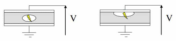
– The corona effect: it appears at the corners of materials placed under an electric field (point effect). This is an ionization of the surrounding air near its corners, see Fig. 8 below.

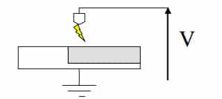
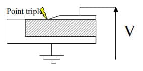
– Surface discharges: discharges originating at the “triple” point metal/insulation/air when there is a defect (drop of water, pollution, dust, etc.) developing on the surface of the insulation. Early problems of insulation degradation are often linked to the presence of water, see Fig. 9 below.

Partial discharges lead to a degradation of materials under the action of various constraints:
- Thermal stress generated locally by the discharge, which can lead to carbonization of the insulation.
- Chemical stress due to degradation products generated by the discharge (mainly ozone, nitrogen oxides and nitric acid).
- Mechanical erosion due to particle projection.
These stresses cause degradation of the material insulating the electrical live parts. When the insulating material is too damaged, a complete electric arc ends up occurring, this is the “initiating” phase. Generally, this phase leads to component failure.
Development of a test bench for partial discharge analysis in our laboratory was first motivated by the need to ensure the life span of customer products, ensure that no partial discharge occurred under the voltage application. A second motivation is to characterize a product when a modification on the manufacturing process or a part replaced by another manufacturer occur. The partial discharge test permit to check the quality of the new parts in comparison to the old one. This kind of electrical test is particularly interesting during preliminary inspection process for failure analysis as it make possible to locate et identify the first hypothesis of defect for example, moreover it is considered as a no destructive test and could allow .
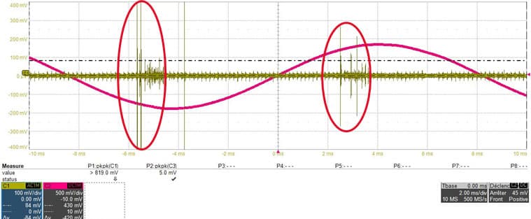
In the example below, Fig. 10 the partial discharge test show the presence of partial discharge when the voltage reach 670Vac. In yellow we can observe the partial discharge peaks while in purple the AC voltage on the device under test.

CONCLUSION
In this paper, we have listed main failure mechanisms attributable during the qualification of connectors at the end of production or after failure during their use. It is necessary to master all the characterization techniques (optical, electrical and material) in order to respond as comprehensively as possible to the needs of our customers.
Indeed there is such a variety of ever more advanced and complex components and just as many potential associated failures. This pushes us to always deepen our knowledge while relying on our past experiences in order to locate defects, dissect failure mechanisms and find the root causes in order to propose the most appropriate corrective actions to support the development of the future components.