by: R. Andersson, M. Bylund, S. Krause, A. M. Saleem and V. Desmaris
Smoltek AB, Gothenburg, Sweden
OUTSTANDING AWARD PAPER BY PCNS ATTENDEES
presented by S.Krause at the 2nd PCNS 10-13th September 2019, Bucharest, Romania as paper 1.2.
Abstract
Complete on-chip fully solid-state 3D integrated capacitors using vertically aligned carbon nanofibers as electrodes to provide a large 3D surface in a MIM configuration have been manufactured and characterized. The capacitance per device footprint area has been studied, as well as its behavior at different temperatures and frequencies. Equivalent series resistance (ESR), breakdown voltage and leakage current have also been measured. The entire manufacturing process of the capacitors is completely CMOS compatible, and in combination with the low device profile of about 4 µm this makes the devices readily available for integration on a CMOS-chip, in 3D stacking, or redistribution layers in a 2.5D interposer technology. Capacitances of ca 350 nF/mm2, ESR of about 100 mΩ, breakdown voltages of up to 25 V and leakage currents in the order of 0.004 nA/nF have been measured.
Introduction
The rise of the Internet of Things (IoT) and the constant demand for miniaturization, increased performance, and more functionality in a single package is constantly pushing the need for integrating more devices onto a single chip. In recent years, the downscaling of components following Moore’s law [1] has not necessarily resulted in a better performance to cost ratio, thus requiring innovation in other areas such as component and system integration. One such example is the 3D and 2.5D [2] packaging technologies. Thus, there is a rising need for on-chip, or in-package, capacitors to be used not only in traditional integrated circuits, but also for integrated components on interposers.
For this purpose, high energy density capacitors have been developed to serve diverse functions in ICs and integrated systems, such as decoupling or RF filtering. Decoupling capacitors act as a charge reservoir and are used to reduce rippling of the supplied power to an IC during spikes of high power demand [3]. However, in order to operate optimally, decoupling capacitors must be placed within a critical distance to both the current load and the power supply, to be effective [4]. Therefore, decoupling capacitors tend to strive for being integrated directly on a CMOS chip for best operation. Further, with the surge of the 2.5D interposer technology featuring embedded components, RF filtering is becoming a very important function requiring capacitors.
For integration, a fully solid-state device is needed, with the parallel plate capacitor being the simplest example. To avoid consuming precious space on the chip surface, clever methods need to be implemented to increase the surface area of the electrode without increasing the footprint area of the device. IPDiA, now Murata, have previously used a method where deep trenches are etched into the Si substrate and atomic layer deposition (ALD) or low pressure chemical vapor deposition (LPCVD) is used to deposit materials to generate a 3D structure with high surface area. Using this approach with 100 µm deep trenches they achieved capacitances of over 500 nF/mm2 [5]. The disadvantage of this method is that it is time consuming and expensive, and the deep trenches will weaken the substrate making it more fragile.
Previous studies have investigated the feasibility of using vertically aligned carbon nanofibers (VACNFs) to enhance the surface area of the electrode of a capacitor, by growing them on a substrate and then depositing Al2O3, HfO2 and ZnO by means of ALD. It was shown that the CNFs were conformally coated [6] and even operating devices with capacitance densities of up to ca 200 nF/mm2 have been demonstrated [7] – [9].
In the present work, we present the fabrication and characterization of fully CMOS compatible capacitors based on VACNFs and ALD deposited dielectrics. Two specific standard dielectric materials, Al2O3 and HfO2, of different thicknesses and in different combinations have been investigated. As a result, truly solid-state, 3D integrable, on-chip capacitors based on CNFs as electrode material [8] – [9] have been manufactured and characterized. The capacitors show specific capacitance in excess of 300 nF/mm2 (per device footprint area), low equivalent series resistance of about 100 mΩ with overall profile height lower than 4 microns, and breakdown voltages up to 25 V. Further, leakage currents of the order of 0.004 nA/nF have been measured which supersedes the leakage current performance of standard polymer-based capacitors used for decoupling purposes.
Experiment
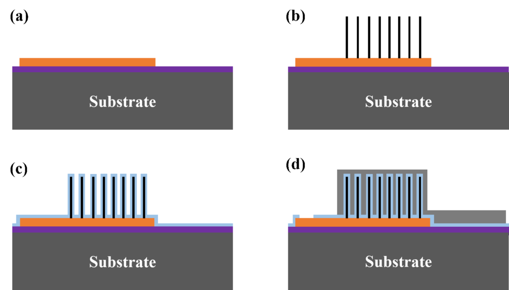
The fabrication process of the solid-state capacitors is shown schematically in Fig. 1. The bottom electrode of the capacitor is first fabricated via standard metal deposition and patterning, Fig. 1a. Electron beam lithography is then used to pattern and then deposit a matrix of catalyst dots. Vertically aligned carbon nanofibers (VACNFs) are then grown directly on the bottom electrode selectively on the catalyst in a DC-PECVD system at 390 °C Fig. 1b. Further details regarding the growth can be found in [10]. The resulting CNF length is 2-3 µm.
By means of atomic layer deposition (ALD), the devices are then coated with a dielectric layer, conformally coating the CNFs as well as the rest of the bottom electrode, Fig. 1c. Different combinations of HfO2 and Al2O3 are used as the dielectric materials in the resulting capacitors, both as pure materials and different stacks of Al2O3/HfO2/Al2O3. Thermal ALD at 250 °C is used for the dielectric depositions.
After the dielectric deposition the top electrode is formed, Fig. 1d. Plasma enhanced ALD at 250 °C is first used to deposit a layer of TiN to ensure fully contacting the sidewalls of the CNFs. A deeper discussion of the effect of TiN deposited via ALD is available in [8]. The bulk of the electrode is then deposited through sputtering. Finally, the dielectric material is opened to allow for probing, Fig. 1 d.
The physical properties of the CNFs after growth are characterized using scanning electron microscopy (SEM), and for the electrical characterization of the capacitors a low frequency vector network analyzer (VNA) is used to do one port S-parameter measurements ranging from 10 Hz to 3 GHz.
The dielectric properties such as breakdown voltage and leakage current are measured using a Keithley 4200SCS Parameter Analyzer.
Results and discussion
Physical properties
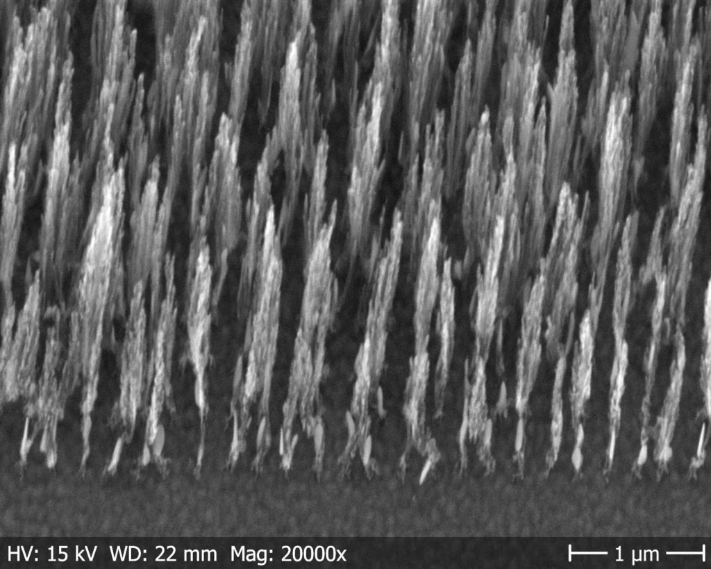
The CNF growth is shown in Fig. 3. The fibers are clearly grown
separated from each other and vertically aligned. The fiber length is only 2 –
3 µm, meaning that the total height profile of the complete device is ca 4 µm.
This makes the capacitors readily available for integration onto a CMOS chip or
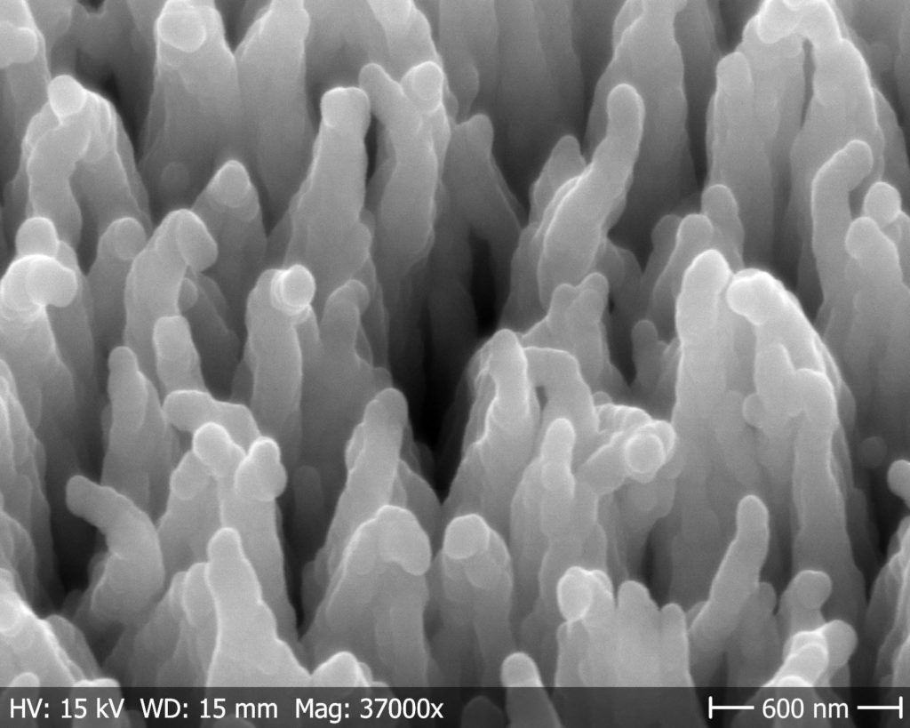
in 3D stacking. Fig. 4 shows the CNFs after the dielectric coating via ALD, the
image showing a coating of Al2O3/HfO2/Al2O3
(5/3/5 nm). The dielectric layer is uniformly covering the individual CNFs.


Capacitance density
Using different dielectric combinations, the capacitance of the CNF-MIMs was investigated by doing one port S-parameter measurements. Fig. 5 shows the resulting capacitance density (per footprint area) for different dielectric combinations. In Table 1, the CNF length for the different dielectric combinations can be seen. As expected, the devices using pure HfO2 show the highest capacitance density at 329 ± 26 nF/mm2. This is due to the higher dielectric constant of HfO2, measured to 19.3, compared to Al2O3, measured to 8.2. Characterization of the dielectric constant is previously done in [8]. The Al2O3/HfO2/Al2O3 stack with thicknesses of 3/9/3 nm shows a higher capacitance density than the one with 3/12/3 nm, since the capacitance is inversely proportional to the dielectric thickness. Finally, the stack with thicknesses of 5/3/5 nm shows an unexpectedly high capacitance density compared to the two other stacks. The higher amount of Al2O3 compared to HfO2 should mean a lower effective dielectric constant of the stack, and thus a lower capacitance. However, the total thickness of the stack is lower for this combination. Also, Table 1 shows that the CNFs on these devices are slightly longer compared to the 3/9/3 nm and the 3/12/3 nm stack, which in turn leads to a larger 3D surface area.
The capacitance behavior at different temperatures was also studied. By using a heated sample holder, measurements were taken at 25 °C, 55 °C, 90 °C, 125 °C, and 150 °C. The change in capacitance density is seen in Fig. 6. Cycling the temperature also showed that the temperature behavior of the capacitors was reversible
The capacitance behavior at different frequencies was also
investigated by studying the impedance of the devices in the frequency range
where the inductive contribution to the impedance can be considered negligible.
A plot of the result from one device with 15 nm HfO2 as dielectric
is seen in Fig. 7.

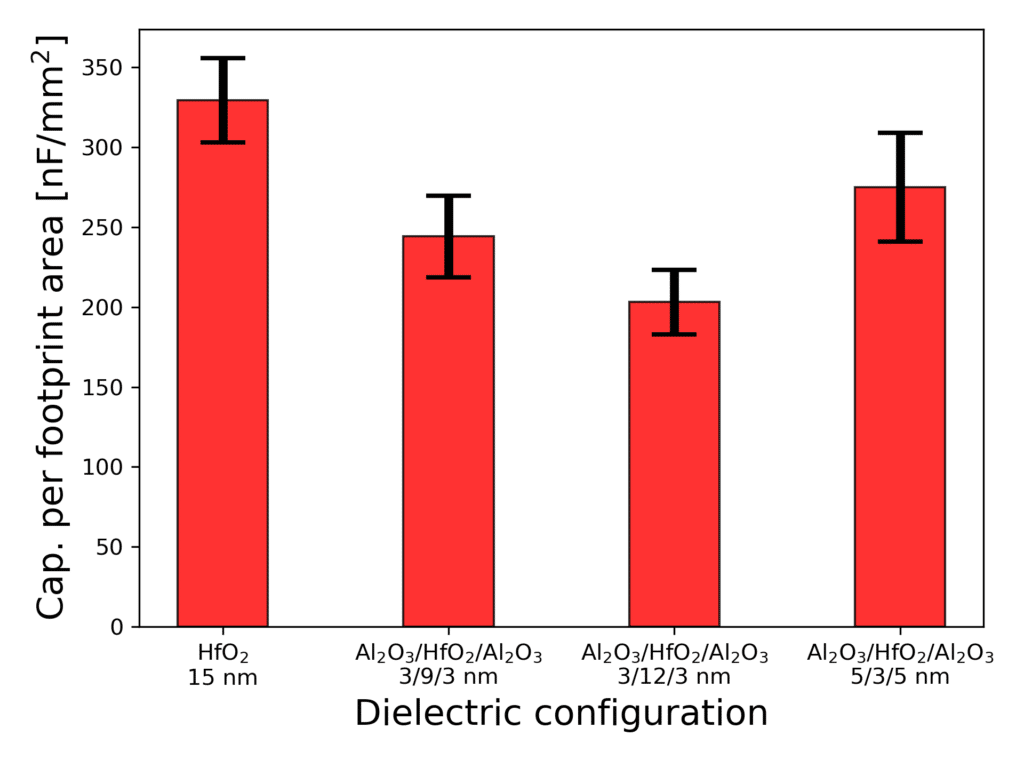

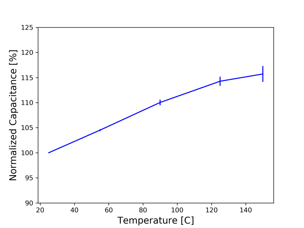

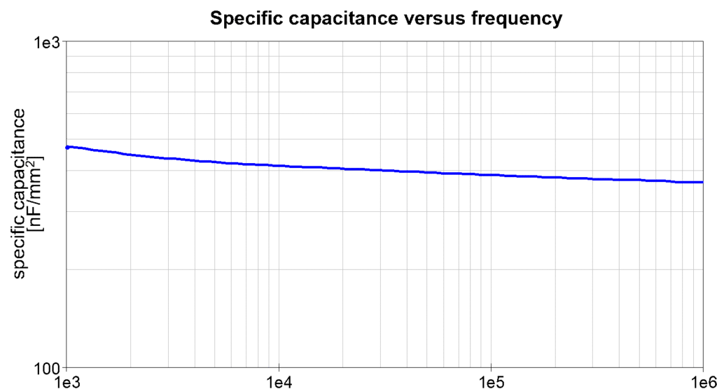
Table 1: CNF length for different dielectric combinations.
| Thickness of layers in Al2O3/HfO2/Al2O3 stack [nm] | CNF length [µm] |
| 0/15/0 | 2.2 |
| 3/9/3 | 2.9 |
| 3/12/3 | 2.5 |
| 5/3/5 | 4.0 |
Dielectric properties
The energy safely stored in a capacitor is limited by the breakdown voltage, which is determined by the dielectric strength of the material. The two different dielectric materials in this work show different properties, Al2O3 provides higher breakdown voltage and HfO2 contributes higher capacitance. Bearing in mind the inherent breakdown–capacitance trade-off, different oxide stacks were investigated to combine the properties of both materials. The resulting breakdown voltage for all dielectric combinations on CNF-MIM devices are shown in Fig. 8. There is an increase in breakdown voltage when using a stack instead of using pure HfO2.
To further investigate the capacitors, measurements of their leakage current were performed at 1 V and at 2 V. The devices were biased for one minute before the leakage current was recorded to avoid transients. The resulting numbers are shown in Table 3, and with a leakage current to capacitance ratio of 0.004 nA/nF, the CNF-based capacitors supersede the performance of polymer capacitors, proving their usefulness.
ESR
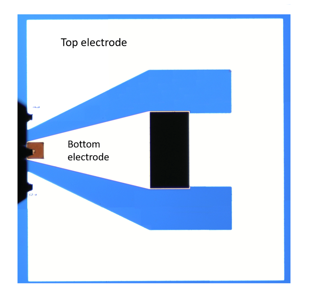
Typically, integrated large capacitance density devices often present relatively large equivalent series resistance (ESR), compared to their discrete counterparts. In this work, the devices needed to be de-embedded to characterize the ESR, since the measurements will contain parasitic impedances that are not inherent to the capacitor itself, but to the metal structure related to probing. To remove this part of the measured data, de-embedding devices were manufactured without any CNFs or dielectric material, i.e. the top and bottom electrodes form a short circuit. These devices are then measured the same way as the CNF-MIM capacitor, and the resulting impedance is subtracted from the measured impedance of the CNF capacitor.
Fig. 9 shows the plotted impedance for a 420 µm x 840 µm device with
Al2O3/HfO2/Al2O3 (3/12/3
nm) as dielectric material after de-embedding the device. The ESR of this
device is extracted as 115 mΩ.

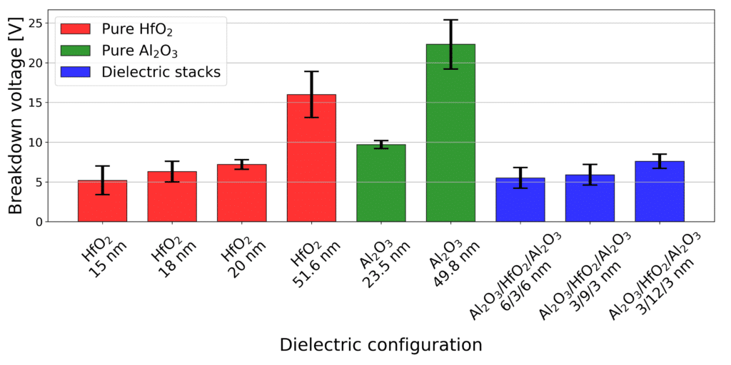

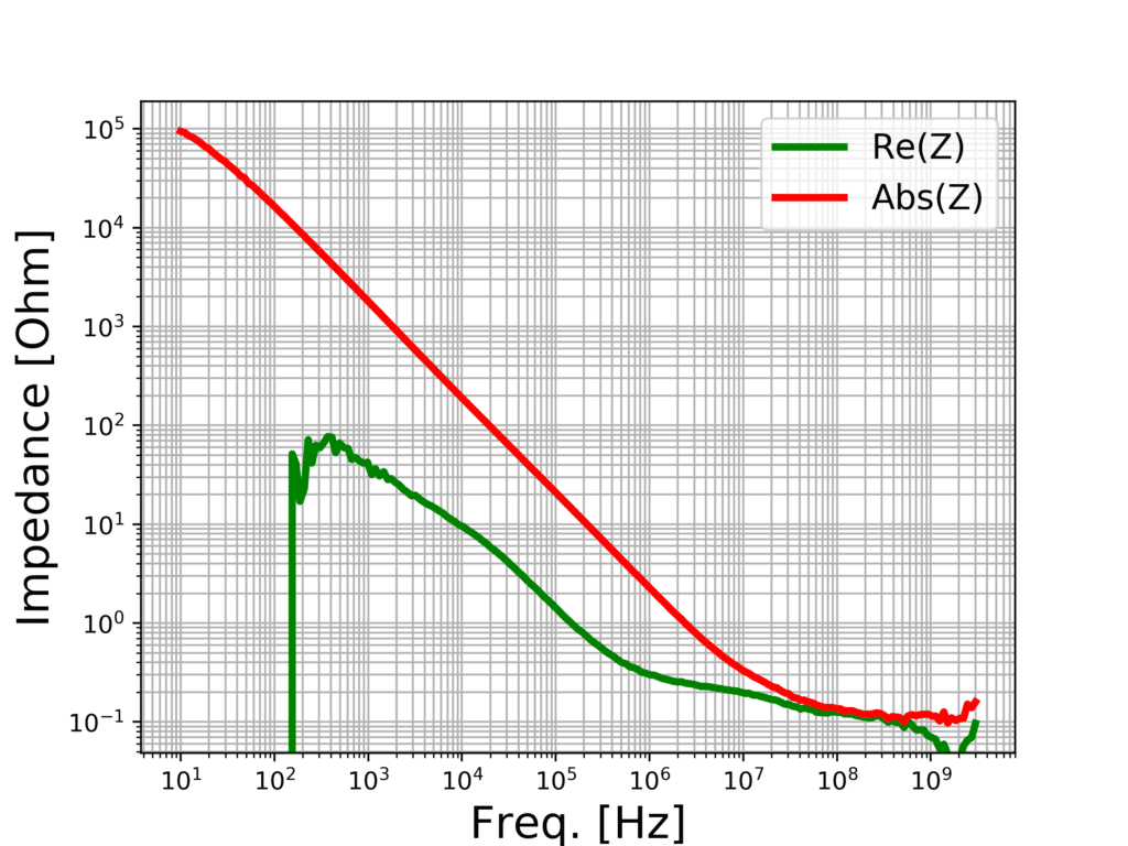
Table 2: measured DC leakage current (DCL) at different voltages
| Measured Cap. [nF] | DCL @1V [nA] | DCL @2V [nA] | DCL/Cap. @1V [nA/nF] | DCL/Cap. @2V [nA/nF] |
| 27.1 | 0.15 | 0.47 | 0.0055 | 0.017 |
| 13.2 | 0.05 | 0.18 | 0.0038 | 0.014 |
| 41.6 | 0.12 | 0.35 | 0.0029 | 0.008 |
| 6.2 | 0.02 | 0.16 | 0.0032 | 0.026 |
| 56.8 | 0.13 | 0.90 | 0.0023 | 0.016 |
| 12.9 | 0.06 | 0.33 | 0.0047 | 0.026 |
Conclusions
Complete on-chip fully solid-state 3D integrated capacitors using VACNFs as electrodes to provide a large 3D surface in a MIM configuration have been manufactured and characterized. The capacitance per device footprint area has been investigated for different dielectric materials, as well as at different temperatures and at different frequencies. Furthermore, the equivalent series resistance (ESR), breakdown voltage and leakage current has been measured. A capacitance density of ca 329 nF/mm2 has been realized from devices with 15 nm of HfO2 as dielectric material. Through de-embedding, the ESR of the devices was found to be around 100 mΩ. The breakdown voltage was measured ranging up to 25 V and followed the expected trends when varying the dielectric thickness and combinations of dielectric materials. DC leakage current was measured, with a leakage current to capacitance ratio of 0.004 nA/nF, superseding the performance of current polymer capacitors.
The entire manufacturing process of the capacitors is completely CMOS compatible, which along with the low device profile of about 4 µm makes the devices readily available for integration on a CMOS-chip, in 3D stacking, or redistribution layers in a 2.5D interposer technology.
References
- G. E. Moore, “Cramming More Components onto Integrated Circuits,” Electronics, vol. 38, no. 8, Apr. 1965, W. Chen, W.R. Bottoms, “Heterogeneous integration Roadmap”, International Conference on Electronics Packaging (ICEP), 2017, pp. 302-305, doi: 10.23919/ICEP.2017.7939380
- M. M. Waldrop, “The chips are down for Moore’s law,” Nature, vol. 530, no. 7589, Feb. 2016, p. 144, doi:10.1038/530144a.
- H. Hu, S. Harb, N. Kutkut, I. Batarseh, and Z. J. Shen, “A Review of Power Decoupling Techniques for Microinverters With Three Different Decoupling Capacitor Locations in PV Systems,” IEEE Transactions on Power Electronics, vol. 28, no. 6, Jun. 20 [1]13, pp. 2711–2726, doi:10.1109/TPEL.2012.2221482.
- M. Popovich, M. Sotman, A. Kolodny, and E. G. Friedman, “Effective Radii of On-Chip Decoupling Capacitors,” IEEE Transactions on Very Large Scale Integration (VLSI) Systems, vol. 16, no. 7, Jul. 2008, pp. 894–907, doi:10.1109/TVLSI.2008.2000454.
- F. Nodet, “Ultra-low ESL and Ultra-low Profile Silicon Capacitor interest in decoupling high-speed IC,” IPDiA.com, 19-Oct-2016. [Online]. Available: http://www.ipdia.com/index.php?page=news&item_id=97. [Accessed: 09-Feb-2018].
- G. A. Malek et al., “Atomic Layer Deposition of Al-Doped ZnO/Al2O3 Double Layers on Vertically Aligned Carbon Nanofiber Arrays,” ACS Appl. Mater. Interfaces, vol. 6, no. 9, May 2014, pp. 6865–6871, doi:10.1021/am5006805.
- A. M. Saleem, R. Andersson, V. Desmaris, and P. Enoksson, “Integrated on-chip solid state capacitor based on vertically aligned carbon nanofibers, grown using a CMOS temperature compatible process,” Solid-State Electronics, vol. 139, Jan. 2018, pp. 75–79, doi:10.1016/j.sse.2017.10.037.
- R. Andersson, A. M. Saleem and V. Desmaris, “Integrated fully solid-state capacitor based on carbon nanofibers and dielectrics,” Proc. 2018 IEEE 68th Electronic Components and Technology (ECTC), 2018, pp. 2307-2312, doi: 10.1109/ECTC.2018.00348.
- A. M. Saleem, R. Andersson, M. Bylund, C. Goemare, G. Pacot, M. S. Kabir, and V. Desmaris, ” Fully solid-state integrated capacitors based on carbon nanofibers and dielectrics with specific capacitances higher than 200 nF/mm2″ Proc. 2019 IEEE 69th Electronic Components and Technology (ECTC), 2019, in press
- A. M. Saleem et al., “Low temperature and cost-effective growth of vertically aligned carbon nanofibers using spin-coated polymer-stabilized palladium nanocatalysts,” Sci. Technol. Adv. Mater., vol. 16, no. 1, 2015, p. 015007, doi:10.1088/1468-6996/16/1/015007.
more 2nd PCNS symposium technical papers can be viewed and downloaded in pdf from EPCI Academy e-Proceedings: