


This article presents a method for thickness reduction of polypropylene (PP) films, used as dielectric materials for capacitors, by ion irradiation, which has a direct effect on device capacitance.
The paper was presented by Shova Neupane, Centre for Industrial Electronics, SDU University of Southern Denmark, Denmark at the 4th PCNS 10-14th September 2023, Sønderborg, Denmark as paper No. 4.2.
Abstract
Polypropylene (PP) films have a wide range of applications, e.g. as dielectric materials for capacitors. In this article, we present a method for thickness reduction of PP films by ion irradiation, which has a direct effect on device capacitance. We show that the thickness of PP layers can be reduced by irradiation with He+ ions and controlled on the nanometer scale by the irradiation dose. The effect of different thin metal film coatings on PP surface was also investigated. The metal coatings were used for two reasons: they function as one of the metal electrodes in the capacitor structure and they minimize sample charging during ion irradiation. Three different metallization materials were investigated: 5 nm Pd40Pt60, 5 nm Au, and 15 nm Al.
We studied two technologically relevant PP films: the thinnest commercially available biaxially oriented polypropylene (BOPP) and spin-coated polypropylene (SC-PP) thin films. The irradiation was done with a focused Helium-ion beam (He-FIB) in a Zeiss Orion NanoFab Microscope at a landing energy of 30 keV with doses in a range of 5.4 x 10⁻⁵ nC/μm2 to 8.07 x 10⁻³ nC/μm2. An atomic force microscope (AFM) was used to analyze the details of surface modification: the surface height of the irradiated regions and surface morphology changes caused by the irradiation. The Al-coated samples demonstrated smaller surface-height reduction compared to the Pt40Pd60 and Au-coated samples. Possible factors responsible for this effect include differences in the thickness and the crystalline-grain structure of the metallization films. Both BOPP and spin-coated PP presented surface ridges at the borders between the irradiated and non-irradiated regions. It can be attributed to the mechanical strain induced by the material modification.
Introduction
New and improved dielectric materials for thin-film capacitors are being investigated and developed to meet the demands of modern advanced electronics. Among them, polypropylene (PP) is commonly used in thin-film capacitors due to several desirable properties, such as high dielectric strength, reliability, and low dissipation factor[1–5]. An approach for increasing device capacitance is decreasing the dielectric thickness, which can be limited by the fabrication process. At present, this process involves mechanical stretching of the material in multiple directions to induce molecular alignment and reduction in the thickness[1–3,6,7]. PP films as thin as 1.9 μm have been fabricated with this process. In previous work on metallized polymethyl methacrylate (PMMA) dielectric films [8,9], we demonstrated that the thickness of these films could be reduced with nanometer precision by He-FIB irradiation, presumably due to chemical decomposition in the bulk of the polymer film. It was also found that the effects of surface sputtering by He-FIB are negligible, and the Pt60Pd40 thin film metallization on the PMMA surface preserves its in-plane features. On the other hand, the irradiation of PMMA samples metallized with Au resulted in delamination, bulging, and perforation of Au films, which was attributed to the accumulation of gases from radiolysis at the Au–PMMA interface[8,9].
In this work, we demonstrate that He-FIB can also be used to reduce the thickness of PP films with nanometer precision and present the influence of different metallization materials on the shrinkage of PP as a function of the irradiation dose. Thin film PP surfaces were metallized with either Pt60Pd40, Au or Al films. The Pt60Pd40 alloy and Au coatings were applied to study the effect of the noble-metal thin films with different crystalline grain structures [8]. Aluminum is, at present, the most used electrode material in PP thin-film capacitors [10].
Materials and methods
Sample Preparation
Two different types of PP thin films were investigated in this study. The first PP sample is the thinnest commercially available extruded BOPP foil with a thickness of approx. 1.9 from Birkelbachfilm GmbH, Germany[11] . To avoid wrinkles during the preparation of the BOPP foils for the Helium irradiation, we have used a special stretching technique, which will be reported elsewhere[12]. The second PP sample was prepared by a spin coating process with a Polos spin coater system. The PP gel was prepared in a 1:1 mixture of o-xylene and toluene using the procedure of Greenbank et al. [13] and spin-coated to 15 mm x 15 mm glass substrate (Prazisions Glass and Optik GmbH, Germany). Polypropylene, o-xylene, and toluene are from Merck, Denmark. The thickness of the spin-coated (SC)-PP films was approx. 170 nm measured by a profilometer (Bruker).

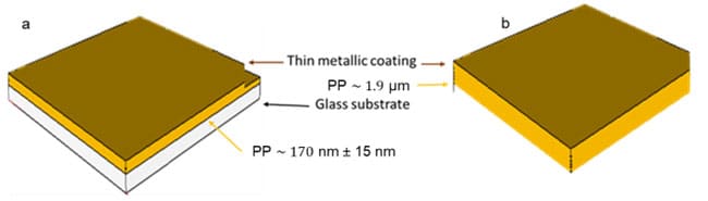
Figure 1a shows the SC-PP sample and Figure 1b represents the extruded BOPP sample. Both BOPP and SC-PP films were coated individually with either 5 nm Pt60Pd40 alloy, 5 nm of Au, or 15 nm of Al to minimize the surface charging during ion irradiation (see summary in Table 1). The 5 nm Pt60Pd40 alloy films were deposited via DC sputtering with a Cressington 208HR sputter apparatus, while both the 5 nm Au and 15 nm Al films were deposited by e-beam evaporation in a Cryofox Explorer 600 physical vapor deposition system. The relatively higher thickness of the Al film was chosen since initial experiments indicated that a thinner film did not efficiently avoid surface charging during irradiation.
| PP Surface | Metal coating |
| SC-PP | 5 nm Pt60Pd40 |
| BOPP | 5 nm Pt60Pd40 |
| SC-PP | 5 nm Au |
| BOPP | 5 nm Au |
| SC-PP | 15 nm Al |
| BOPP | 15 nm Al |
A Zeiss Orion Helium-ion Microscope (HIM) was used for both the irradiation with He+ ions and for imaging the surface of the samples. The metallized BOPP and SC-PP films were irradiated at a landing ion energy of 30 keV. The beam current for all the irradiations was in the range of 0.9-1.0 pA with a beam dwell time of 0.2 µs, spot control 4, and a single raster scanning mode with multiple passes. In order to investigate the influence of the dose on the surface height, different areas were exposed to different He+ ion doses ranging from 5.40 x 10⁻⁵ nC/µm2 to 8.07 x 10⁻³ nC/µm2 [8,9] (the doses were applied in an increment order as presented in Table 2). The distance between two irradiated areas was 40 µm to avoid possible interference between neighboring areas. HIM image in Figure 2 shows nine 10 x 10 µm2 irradiated areas arranged in a 3 x 3 array.
| Pattern number | Dose (nC/µm2) |
| 1 | 5.40 x 10⁻⁵ |
| 2 | 3.21 x 10⁻⁴ |
| 3 | 5.88 x 10⁻⁴ |
| 4 | 8.55 x 10⁻⁴ |
| 5 | 1.66 x 10⁻³ |
| 6 | 3.26 x 10⁻³ |
| 7 | 4.06 x 10⁻³ |
| 8 | 8.07 x 10⁻³ |
| 9 | 5.40 x 10⁻⁵ |
The starting dose was used again at the end to ensure the reproducibility of the dose. In Figure 2 the irradiated areas appear darker than the surroundings, and the darkness increases with increasing the irradiation dose. All the irradiated surfaces observed with the He+ ion microscope are very similar for both extruded BOPP and SC-PP. Therefore, only one representative image of a 5 nm Pt60Pd40 coated SC-PP surface He+-ion image is shown in Figure 2. AFM topography measurements were made with a Nanosurf FlexAFM system using a non-contact mode AFM probe 190Al-G from Budgetsensors. The images were processed with the software Gwyddion [14].


Results
Polypropylene surface analysis
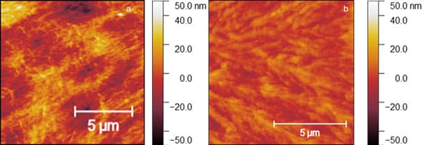
Prior to the metal coating, the BOPP and SC-PP sample surfaces were characterized with AFM (Figure 3). The surface morphology and roughness of the two PP films are significantly different. The BOPP surface is comparatively smooth with lower surface RMS roughness than the SC-PP. The local RMS surface roughness of the BOPP surface is 5 nm (Figure 3a). In contrast, the SC-PP surface RMS roughness is 10 nm (Figure 3b).

Helium ion irradiation
Upon metallization the PP samples were irradiated with He-FIB according to the doses provided in Table 2. In Figure 4, the AFM images show the irradiated areas as depressions as compared to the non-irradiated surroundings. Figures 4a and 4b are AFM images of the samples with 5 nm of Pt60Pd40-coated SC-PP and 5 nm Pt60Pd40 coated BOPP. The depth profiles obtained across the irradiated area up to the non-irradiated show depressions with depths of 25 nm ±5 nm and 20 nm ±5 nm, respectively. There is no indication of surface delamination, cracks, or gas accumulation around the irradiated areas. The SC-PP and BOPP samples metallized with 5 nm of Au are presented in Figure 4c and 4d, respectively.
Previous studies performed on PMMA coated with 15 nm of Au showed that the metallization might form a barrier to the permeation of gases leading to delamination and bulging of the Au films [8,9], but such delamination and bulging are not observed with the SC-PP and BOPP samples. The absence of delamination and bulging is most likely due to the thinner 5 nm Au layer deposited on SC-PP and BOPP samples, which are also rougher than the PMMA (less than 5 nm). This will be addressed more thoroughly in a follow-up study. The 15 nm Al metallized surface showed similar patterning features for both SC-PP and BOPP, as shown in Figures 4e and 4f. However, the depths are relatively lower than those obtained for the Au and Pt60Pd40 coatings. When using a dose of 5.4 x 10⁻⁵ nC/µm2 on the Al surface only minor height variations (less than 10 nm) were observed. Therefore, Figures 4a and 4f present the results of an increased He+ ion dose of 3.21 x 10⁻⁴ nC/µm2. The patterns created with 5.4 x 10⁻⁵ nC/µm2 are presented in the supplementary material image S2. The possible reason for this height difference could be the thickness of the aluminum, which was three times thicker than the Au and Pt60Pd40 layers.


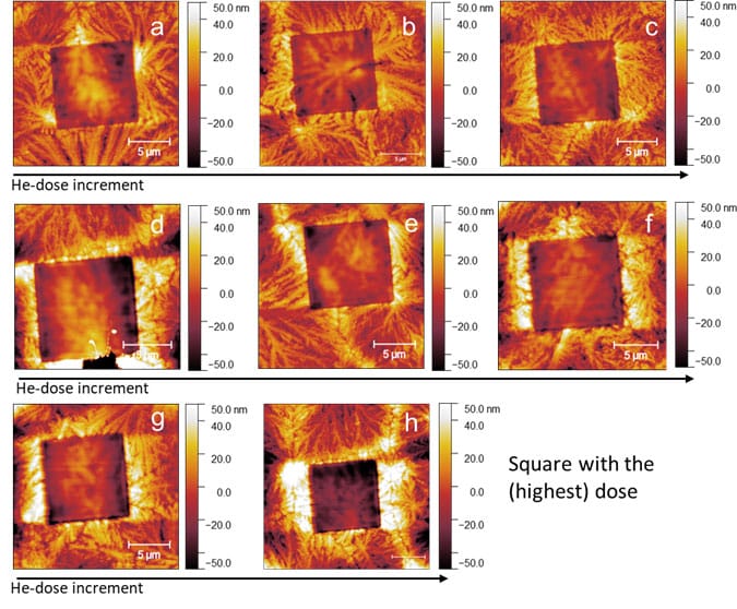
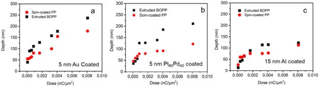
Figure 5 shows AFM images of He+ ion irradiation dose-dependent square patterns on SC-PP surface metallized with 5 nm Pt60Pd40. Pattern (a) is the result of the first applied dose. i.e. 5.40 x 10–
5 nC/µm2, which is the same as Figure 4a. It can be observed that the pattern depth increases with increasing irradiation dose. The depth dependence with dose is shown in Figure 7.
The contrast in the border between irradiated and non-irradiated areas starts to appear more pronounced after the fourth dose, i.e., from 8.55 x 10⁻⁴ nC/µm2. The sharp edges of the focus He+ ion differentiate the suppression of the PP layer. Also, it shows that the surface structure slightly changed, yet the spherulite structure inside the irradiated pattern is visible. Similar AFM images were recorded on both the 5 nm Au-coated surface and the 15 nm Al-coated surface. These results are presented in supplementary material Figures S1 and S2, respectively.

A similar measurement was done on the BOPP surface with the same physical parameter as the SC-PP surface. Figure 6 shows AFM images of the BOPP surface metallized with 5 nm Pt60Pd40 alloy after ion irradiation. The He+ ion and the AFM images show similar surface characteristics for both BOPP and SC-PP samples i.e. no sputtering effects appeared up to the third dose, and only the polymer shrinkage was observed. Surface ripple and more clear contrast appears after the fourth dose up to the highest applied dose. Similar measurements were done on BOPP surfaces with 5 nm of Au and 15 nm of Al. These are presented in the supplementary material as Figure S3 and S4, respectively.

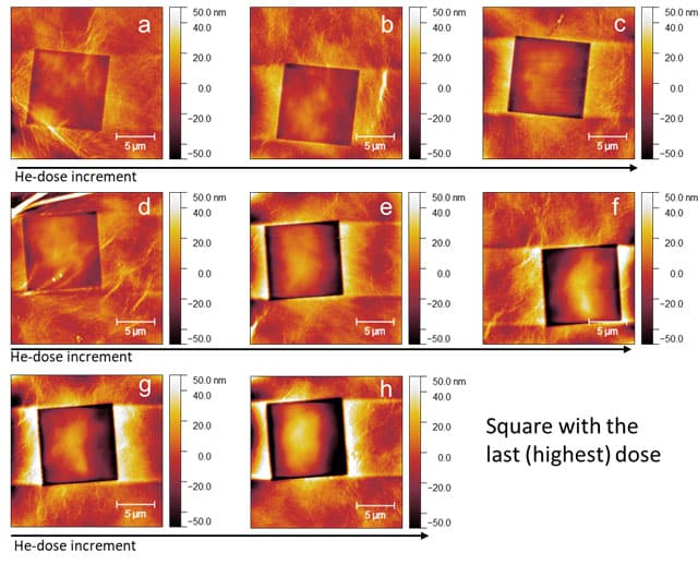
Figure 7 represents the depth-profile of the irradiated regions as a function of the dose for the SC-PP and BOPP samples. The baseline to calculate the edge effects was measured from the non-irradiated surface up to the He+ irradiated area (inside the squares). Pattern edge depth was represented as the average height difference of the five cross-sections of all sides of the square edges. In Figure 7 all curves show a steep increase in depth at low doses followed by a saturation for higher doses. However, compared to the samples coated with Au (Figure 7a), the samples coated with Pt60Pd40 (Figure 7b) and Al (Figure 7c), show a more distinct saturation. Presumably, the gold-coated samples form a stronger barrier to the permeation of gases and hence hinder shrinkage of the polymer. Surprisingly, in Figure 7b, the initial rate for the thin spin-coated PP is similar to the thick extruded BOPP. We would expect a lower surface-height reduction rate for the thinner samples due to the significantly smaller volume of material involved in the shrinkage process. It could be an indication that the structure of the polymers has an effect on the material’s response to ion irradiation exposure. In Figure 7c, both SC-PP and BOPP samples show lower shrinkage compared to Figures 7a and 7b.

Conclusions
In this work we demonstrated that the thickness of metallized extruded (BOPP) and spin-coated (SC-PP) polypropylene (PP) films can be reduced and controlled with He+ ion irradiation on a nanometer scale.
The gold-coated samples seem to have a stronger barrier to the permeation of gasses which leads to slower shrinkage. The thicker Al coating seems to have a strong impact shielding the polymer against the irradiation. Additional factors such as differences in the crystalline-grain structure, can also influence the materials’ response to the He+ irradiation.,.
We found that the thickness reduction is higher for BOPP films than for SC-PP films. It is presumably due to the smaller volume of material involved in the shrinkage process of the SC-PP films since most of the electronic energy losses and the nuclear collision events are localized in the underlying glass substrate. Further investigations are needed to clarify the contributions of structural, morphological, and chemical factors on the observed effects.
Declaration of Competing Interest
The authors declare that they have no known competing financial interests or personal relationships that could have appeared to influence the work reported in this paper.
Supplementary material
Supplementary material is available.
Data availability
Additional data will be available upon a reasonable request.
Acknowledgments:
The authors acknowledge the Villum Foundation with project no. 40724 for financial support.
References
[1] Zha JW, Zheng MS, Fan BH, Dang ZM. Polymer-based dielectrics with high permittivity for electric energy storage: A review. Nano Energy 2021;89. https://doi.org/10.1016/j.nanoen.2021.106438.
[2] Montanari D, Saarinen K, Scagliarini F, Zeidler D, Niskala M, Nender C, et al. Film Capacitors for Automotive and Industrial Applications. Proceedings CARTS USA 2009, 29th Symposium for Passive Electronics, March, Jacksonville, FL.
[3] Maddah HA. Polypropylene as a Promising Plastic: A Review. American Journal of Polymer Science 2016;6:1–11. https://doi.org/10.5923/j.ajps.20160601.01.
[4] Gahleitner M, Tranninger C, Doshev P. Heterophasic copolymers of polypropylene: Development, design principles, and future challenges. J Appl Polym Sci 2013;130:3028–37. https://doi.org/10.1002/app.39626.
[5] Hsieh CT, Pan YJ, Lin JH. Polypropylene/high-density polyethylene/carbon fiber composites: Manufacturing techniques, mechanical properties, and electromagnetic interference shielding effectiveness. Fibers and Polymers 2017;18:155–61. https://doi.org/10.1007/s12221-017-6371-0.
[6] Wu CL, Zhang MQ, Rong MZ, Friedrich K. Tensile performance improvement of low nanoparticles filled-polypropylene composites. Composites Science and Technology 62 (2002) 1327–1340.[11]
[7] Fan Y, Niu Z, Zhang F, Zhang R, Zhao Y, Lu G. Suppressing the Shuttle Effect in Lithium-Sulfur Batteries by a UiO-66-Modified Polypropylene Separator. ACS Omega 2019;4:10328–35. https://doi.org/10.1021/acsomega.9b00884.
[8] Chiriaev S, Tavares L, Adashkevich V, Goszczak AJ, Rubahn HG. Out-of-plane surface patterning by subsurface processing of polymer substrates with focused ion beams. Beilstein Journal of Nanotechnology 2020;11:1693–703. https://doi.org/10.3762/BJNANO.11.151.
[9] Tavares L, Chiriaev S, Adashkevich V, Taboryski R, Rubahn HG. Height patterning of nanostructured surfaces with a focused helium ion beam: A precise and gentle non-sputtering method. Nanotechnology 2020;31. https://doi.org/10.1088/1361-6528/ab6679.
[10] Buhrkal-Donau S, Bordo V, Ebel T, A way to High Voltage Polymer Aluminium Electrolytic Capacitors. 2021. https://passive-components.eu/a-way-to-high-voltage-polymer-aluminium-electrolytic-capacitors/
[11] Birkelbach Kondensatortechnik GMBH. Polypropylene.
[12] Odysseas Gkionis-Konstantatos WGSNTELTavares. Enhanced Heat Dissipation Property for Metallized Polypropylene Film Capacitors. Nordic Polymer days 2023, Copenhegan: 2023.
[13] Greenbank W, Ebel T. Layer-by-layer printable nano-scale polypropylene for precise control of nanocomposite capacitor dielectric morphologies in metallised film capacitors. Power Electronic Devices and Components 2023;4:100025. https://doi.org/10.1016/j.pedc.2022.100025.
[14] Klapetek P, Neˇ D, Anderson C, Anderson C. Gwyddion user guide 2009.
The full scientific paper has been published by Power Electronic Devices and Components and available at https://doi.org/10.1016/j.pedc.2023.100046