


This paper describes the physical background of the voltage-dependent capacitance of class II Multilayer Ceramic Capacitors (MLCC) and present models for this dependency.
The paper was presented by Chris Muter, TT Electronics, UK at the 4th PCNS 10-14th September 2023, Sønderborg, Denmark as paper No.2.4.
Thick film printing is and has been the backbone of surface mount resistor products for many years. Although this technology is widely utilised for printing on ceramics, there are a multitude of demanding and power-dense applications that could benefit from this technology.
These high-power applications exploit printing on steel – which is less widely known but offers market leading advantages. This white paper explores thick film technology for more challenging applications i.e., high temperature & high vibration / shock to help designers realise the full capabilities of using this technology.
Introduction
It is very common to have a ceramic substrate in electronic components. In fact, nearly all chip resistors and hybrid modules incorporate conductive / resistive films printed onto ceramic substrates, usually Al2O3 (Alumina) or AlN (Aluminium Nitride). This white paper looks at what happens if the substrate is changed. Specifically, exploring what happens if the substrate material is changed from ceramic to steel.

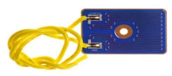
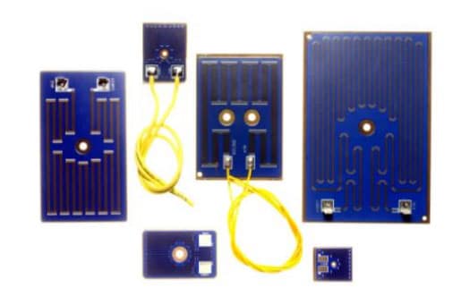
The basis of TFS (Thick Film on Steel) technology is derived from thick film printing technology. Thick film technology is well established and prolifically used within the electronics industry. It appears in devices such as micro hybrid circuits / modules, sensors, power resistors, heating elements and integrated passive devices. See below, figure 1, for an example.
The basic manufacturing process relies on screen printing conductive & resistive inks through stretched screen meshes onto a substrate. Screen printing, the basic concept of this process, has been in existence in some form for thousands of years.
When the technology was first introduced to the electronics industry, it became one of the most dominant manufacturing processes in the 1950’s – resulting in the acceleration of miniaturisation in electronic devices. Thick film thicknesses range from microns to a couple of hundred microns.
Thick Film on Steel technology
You can view this technology as a more resilient PCB (Printed Circuit Board) technology as the films are printed and then fired at high temperatures (typically 700°C to 900°C) usually onto a ceramic substrate. The ceramic provides insulation to the conducting tracks printed on the top forming a circuit.
However, the films are fired at such high temperatures that the finished circuit can be exposed to higher temperatures and remain intact – unlike PCB technology. This lends the technology perfectly toward applications where reliability and high temperature robustness are critical factors.
At first glance, this may not even seem possible due to steel itself being a conductor and therefore unable to provide the electrical insulating properties that ceramic can. However, this can be overcome with the use of thick film dielectric materials. The materials on the TFS product have been matched and optimised to allow superior adhesion properties even under extreme stress. As shown in figure 2 a component has been bent past 90° and still displays good adhesion of dielectric materials, with some minor cracking from the edges only. The cracks will still occur at the corners due to very high stress but maintaining adhesion across the substrate with such a severe bend is only possible due to the great TCE (Temperature Coefficient of Expansion) match of the base dielectric material and the steel.


By first printing layers of thick film dielectric material over the steel, you can create an isolated plane to print a circuit comprised of conductive / resistive thick film inks. This results in a Dielectric Withstand Voltage (DWV) breakdown of >2.5kVDC, this can be optimised and increased based on product requirements. Once an electrically insulated layer is printed, dried and fired, conductor layers and resistor layers are then added.
The materials used are processed in the same way as the dielectric. Finally, an overglaze is printed over the resistor ink to ensure environmental protection and stability of the resistor element – in some applications multiple layers can be printed to provide DWV breakdown on the top of the product as well as the base of the product. The technology also has a failsafe (open circuit) where it will still maintain a minimum 1kv Dielectric withstand after failure. The construction of the materials and specific design also allows for the technology and product to be UL508C qualified.
Another example of the technology displaying suitable robustness and design for purpose is its ability to withstand thermal cycling of -55°C to +155°C, 5minute dwell at each temperature, then change to temperature performed in <3minutes. A test of 1000cycles has been performed with no effect to Dielectric Withstand Voltage breakdown, no effect on Resistance value, and no physical breakdown or visible degradation of the part. It is worth noting that this testing was performed with no power to the components.
Thermal Interface Materials (TIMs)
There are many options when it comes to Thermal Interface Materials (TIMs) they include but are not limited to Thermal Pads, Thermal compound or grease, thermally conductive adhesive tapes, Phase change materials (waxes), and thermally conductive epoxies.

The effectiveness of the various materials is measured in w/m-K and has a huge range; typically, these fall in the order of around 1w/m-K to 15w/m-k but can go much higher such as in diamond embedded TIMs with a thermal conductivity of ~1800w/m-k. As with all applications this comes down to cost and requirements. The effectiveness will also be hindered by the other materials involved in the process. [1]
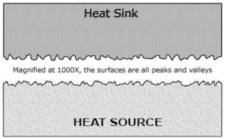
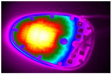
In the process of producing this product, a substrate with comparable thermal conductivity compared to Alumina ceramic i.e. Al2O3 (Alumina) at ~25-30W/m-K. A good thermal interface is critical in getting the most out of the product. The performance of the product is hampered if a good thermal interface between product and heatsink is not achieved, as the surface finish of these is never going to be 100% coplanar. This is shown in figure 3.
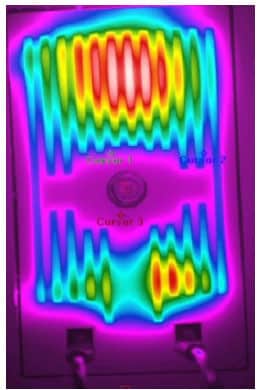
Both figs 4. and 5. are a WDBR3 product heated to a steady state on a fan cooled heat sink, mounted with the same torque, and in the same test conditions. As is evident from the above there is a clear advantage to using a suitable Thermal Interface Material. Figure 4 shows good & even heat distribution of heat across the part as would be expected, with a focal hotspot on one side of the resistor away from the solder pads positioned at the bottom of the image. Figure 5 shows how the distribution of heat is more erratic, a more focused hotspot in the centre of the top of the component shows it is not dissipating heat as evenly, there is an additional hotspot near the solder pads which shouldn’t be present.


Graph 1.1 shows the outcome of a temperature rise of a component with a TIM vs a component without a TIM. As is evident the component without a TIM reaches from ambient temperature to a peak much quicker, in this example approx. 10seconds to reach a much higher temperature, in this case the test was turned off to avoid thermal runaway. The component with a TIM takes ~60seconds to reach a much cooler temperature. This shows visually the key importance of selecting a suitable Thermal Interface Material. As shown a significant difference can be seen in the temperature, around 40% higher in 1/6th of the time, with the test having to be stopped to avoid the part failing.
The heatsinking capability results in a much more power dense component. Not only is it now an incredibly power dense structure, but it is also planar contributing very low inductance (typically <6μH) than in stark contrast to the high inductance usually found in the heavier and bulky wirewound equivalents. It is for these reasons, in addition to other reliability advantages, that this resistor technology is used in some of the most demanding applications.
Established Applications of Thick Film on Steel Technology
There are many well-established applications of this technology since the technology itself is not new. Therefore, within this white paper we will cover these existing applications but also explore the lesser-known applications where thick film on steel technology (TFS) can be advantageous.
Dynamic Braking Systems – Military and Civil Aerospace
Resistors take many shapes and sizes depending upon the chosen technology. Thick film on steel however lends itself to being one of the most power dense resistor technologies on the market today. Therefore, the technology has proved highly successful in many power critical applications across numerous markets – most notably the military and civil aerospace industry.
TFS is one of the most power dense resistor technologies available on the market. When correctly implemented, it can handle large amounts of power for its given size – as explained in the introduction of this white paper. Due to this massively increased power density, it is of little surprise that in comparison with an equivalent wirewound power resistor, it weighs substantially less.
Weight is of key importance for the aerospace industry as reductions lead to greater efficiency and less fuel, ultimately increasing the range of the aircraft or vehicle. Furthermore, the construction of the technology is, by design, planar. Thus, parasitic effects that you may encounter when designing with high power resistors, such as unwanted inductance for fast di/dt switching applications, means that the comparative contributing switching inductance from the WDBR TFS resistor solution will be also significantly less than the equivalent wirewound resistor solution.
These key advantages have been hard to ignore for both the military and civil aerospace sectors, with strong adoption of the technology in both. This is also a key technology which supports worldwide leading industry trends such as “More Electric Aircraft”1. This is just one example where TFS technology really helps put designers ahead in some of the most challenging aircraft applications including control of flight surfaces and inflight refueling hose drum systems. With the rising trend towards more electric aircrafts, the need for TFS technology in both military and civil applications is likely to increase.
More Electric Aircraft is EMEA’s industry-wide quest to optimise aircraft performance, decrease operating and maintenance costs and reduce gas emissions.[3]
Dynamic Braking Systems – Industrial
Most industrial processes involve precise movement usually generated by a motor. Small motors are easy to control and have very little residual energy when turned off. However, heavier industrial applications such as; lifting, pumps, HVAC and electric vehicles demand larger motors which in turn demand more challenging control factors and considerations.

When power to a large motor is cut, the integral moving parts of the motor have built momentum due to the large size and weight of their components. This means that residual kinetic energy from the system eventually dissipates as heat energy as the motor gradually comes to a stop.
However, in some applications it is not ideal or practical to have excess kinetic energy within a system. For example, many automated processes rely on moving material up to, and not past, a certain point – i.e. in a lift system. Therefore, Dynamic Motor Braking resistors play a huge role in dissipating this unwanted and unusable excess kinetic energy. By connecting across the motor, they act as a load powered by the motor, converting the kinetic energy into heat energy dissipated by the dynamic braking resistor.
Civil Aerospace
In the previous section we covered dynamic braking resistors for industrial applications. We explored why heat energy is a waste product which has to be safely dissipated in these applications. However, did you know that there are other applications which can put this heat energy to good use?

A prime example of this is heaters on civil aircraft where safety is paramount. For this reason, conventional cost-effective coil elements are not permitted in the design. This is due to the product not being guaranteed for high reliability and / or not incorporating any failsafe mechanisms. As you can imagine, a fire onboard an aircraft by fault or overload of an electrical heater element would be potentially catastrophic. For these reasons more reliability and specialist solutions must be qualified and successfully implemented.
Another example application for this in aerospace is as an Electronic Braking Actuator Controller (EBAC) this replaces a traditional technology of brake by wire, this is known as electrically actuated brake-by-wire technology. This allows for faster installation, easier replacement of parts, reduction in operating costs, quicker response times, significant weight reduction, more efficient brake wear to name just a few.
As detailed in figure 8, there is less required to make an efficient braking system using the TFS technology and ultimately less to go wrong. Hydraulics are heavy and more prone to failure.


Braking Resistor – Military Applications
The technology has resistance to thermal shock, resistance to extreme vibration, harsh environments, high temperature operation, a combination of these properties lend themselves to some of the harshest applications, including as dynamic braking resistors enabling more electrification of military land & air vehicles. i.e., dynamically braked aircraft flight surfaces.
Earlier in this white paper the TFS construction technology was described in some detail as being a material stack including a steel substrate, dielectric material, resistor material and an overglaze. This is not too dissimilar to a PCB. Thus, TFS technology allows other components to be integrated onto the substrate, just like a PCB, something which is not easily achieved with other technologies. For example, thermal cut outs, thermistors and fuses can be added for protection of the heating resistor to guard it from bearing too much load and consequently failing. As the protection circuitry can be integrated onto the same substrate as the resistor, major space saving is achieved. TFS technology leads the way in offering weight and space saving benefits over other competing technologies, due to its planar construction it is more suited to fitting in narrow size envelopes. This additional space saving is just another reason why aerospace customers choose to adopt the technology – paying them dividends over the life of the aircraft / payload.
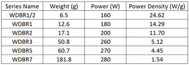
The tables below (Table 1.1 and Table 1.2) display the weight to power handling available with a TFS product vs a standard wirewound product. The average power to weight ratio being 0.42W/g for the wirewound series. This ranges drastically as can be seen in Table 1.1, but the outcome of this is WDBR technology vs Wirewound, the WDBR has up to 58x the power density. Further visual effect of this is evident in Graph 1.2 highlighting the vastly superior power density.
WDBR TFS Powers & Weights:

Wirewound Powers & Weights:


Comparison of WDBR TFS to Wirewound Power Density & Weight Benefits:

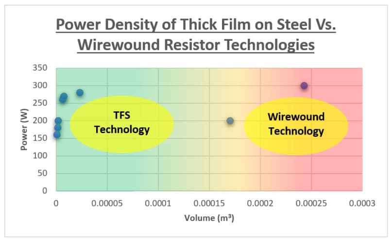
Graph 1.2 as above details a great visual representation of the advantages of TFS Technology vs Wirewound Technology. When combining the above graph with Table 1.1 and 1.2 the difference in the power densities of the two technologies is obvious to see.
Heating Elements – Medical
As discussed, TFS technology lends itself to many applications in both the industrial and Aerospace and defence markets. However, the benefits of TFS are also ideal for applications in the medical industry where performance failure is not an option. The medical industry demands reliability and precision in temperature-controlled environments that TFS can consistently deliver with robust construction technologies, high thermal conductivity, and low thermal inertia.
Applications that require this technology include anesthesia delivery systems, respiratory therapy devices such as ventilators, blood and intravenous (IV) fluid warmers and transfusion equipment.
Emerging applications of Thick Film on Steel Technology
It has long been known that thick film on steel technology has proven successful in dynamic motor braking. In studying the use of TFS in these applications, two emerging themes present themselves. Firstly, the technology is still not widely known and therefore has yet to be adopted in the wider market. Secondly, that the technology has a lot more to offer in increasingly power dense, high reliability and demanding applications.
Additional application of Dynamic braking system in Oil and Gas highlights a new application of the technology which pushes boundaries and proves that TFS technology is more than qualified for use in other sectors.
Dynamic Braking Systems – Oil & Gas
A collaboration with an oil and gas customer, with an aim of increasing the reliability of their electrical systems. The common saying “time is money” could never be truer in the oil and gas industry. Hence the benefits of finding such a solution are worth their weight and more in gold.
WDBR TFS High Temperature & High Shock Robustness
The results of this collaboration and implementation of TFS technology have surpassed all expectations. It is thus a real testament to how robust technology is and how much more untapped capability is has to offer.
What was conducted?
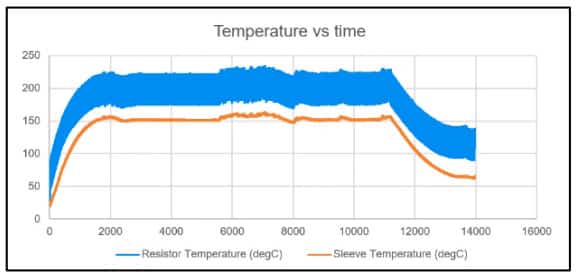
A sample of 6 custom TFS elements were subjected to 100,000 shocks at a level of 250G in a chamber heated to 150°C whilst also being powered with 1.15kW with a duty cycle of 15%.
The Results: High Temperature & High Shock Test Data
The TFS technology proved to be superior throughout high temperature and high shock testing, showing no signs of degradation after the aforementioned test criteria. This can be seen within Graph 1.3 by the plate temperatures remaining consistent throughout the shock testing. Electrical performance was maintained, and the resistors did not fuse or thermally run away with a ΔR% of less than 0.5% after cyclic loading was applied and component returned to pre-testing temperatures. The sleeve temperature is the solid line, the cooler temperature, having a consistent high of ~150°C with the duty cycle of the product and the max observed temperature of the product is ~225°C.
The shock test being performed at 250G greatly surpasses any standard requirements against MIL-STD-810H, the peak for this for any functional aircraft/flight equipment being only 40G, and that of any ground equipment being 75G. [4] The fact the technology can withstand shock much greater than required demonstrates its robustness and durability.

Within the oil and gas industry reliability is of paramount importance, particularly through shock, vibration, and high temperature testing. This means that quite often industrial components cannot be used due to inferior reliability.
The test not only demonstrates that TFS technology is more capable than we currently understand, but also that it is perfectly placed for demanding high power, high shock and high reliability applications.

Conclusion
Thick film on steel technology has more to offer the global electronics industry than most designers may realise, the capabilities highlighted for the standard product are likely just the tip of the iceberg and is constantly evolving and adapting to research into higher power capabilities, better power dissipation, and more extremes of heat and shock can likely be survived.
In this paper the benefits of TFS are highlighted and how the technology can be successfully utilised to help solve some of the toughest challenges in the industrial, medical, aerospace and defence markets.
Acknowledgements
- Dr. Swee gim NG (PhD)
- Callum Riches
References:
[1] https://luminusdevices.zendesk.com/hc/en-us/articles/4412008045069-Thermal-How-do-I-pick-a-TIM-
[2] https://blog.marianinc.com/blog/an-introduction-to-thermal-interface-materials
[3] https://moreelectricaircraft.com/
[4] https://www.trentonsystems.com/blog/mil-std-810-shock-testing-overview-method-516.8