


The paper compares two ways to increase the robustness of assembly against ECM electrochemical migration. In the paper, we underline some challenges in gap cleaning. We describe state-of-the-art methods of cleaning process control and diagnostics, which move the cleaning process from randomly controlled to very safe with stable results.
The paper was presented by Vladimir Sitko, PBT Works s.r.o., Rožnov pod Radhoštěm, Czech Republic at the 4th PCNS 10-14th September 2023, Sønderborg, Denmark as paper No. 3.1.
Abstract
Reliability is the primary concern of electronic assemblies in many applications today. Demands for a long lifetime and the ability to work in a harsh environment have become essential for electronic equipment.
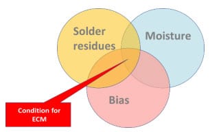
One primary risk for all electronic assemblies is electrochemical migration (ECM). Conditions that trigger the ion movement are bias, ionic active impurities, and moisture. Depending on the intensity of those three factors, the damage starts slowly or faster. Because of hardly predictable environmental moisture conditions, it is not easy to predict when the ECM can start. The paper compares two ways to increase the robustness of assembly against ECM.
The often applied is the protection of assemblies by separating the ionic residues (generated during assembly) against moisture. We describe present methods of industrial application of so-called NO-clean technology. We show current testing methods and calculations of the risk of ECM for such an approach.
The other method for increasing the robustness is cleaning. By cleaning electronic assemblies, we understand a thorough cleaning. The most critical parts of the assembly are the areas between poles. For most packages, this means perfectly cleaning the space (gap) under the component. The challenge of cleaning the gap under the component causes a significant difference between the cleaning process, which was sufficient 15-20 years ago, and which needs to be strictly controlled now.
In the paper, we underline some challenges in gap cleaning. We describe state-of-the-art methods of cleaning process control and diagnostics, which move the cleaning process from randomly controlled to very safe with stable results.
Protection of electronic assemblies against electrochemical migration (ECM)
Today, a significant portion of electronic assemblies needs to work highly reliably. Also, electronics are submitted to very harsh environments in many applications. There are different risks for assembly reliability. However, in this article, we speak about electrochemical migration only (ECM). ECM can seriously disturb the function of assembly of cause a fatal damage. Metal ions can be generated and transferred only if three conditions are fulfilled.
Conditions for ECM
- Electric field (applied voltage)
- Moisture
- Presence of any accessible dissociable compounds which can release ions
All difficulty is that the necessary amount of moisture and the necessary amount of ionic species is hard to determine. Therefore, Electrochemical migration is, in many cases, unpredictable.
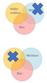
There are two ways how to limit the risk of ECM:
- protection of critical places of assemblies against moisture – no-clean technology
- Protection by no clean flux system, the ionic active residues should be covered by a resin layer. This layer should prevent the penetration of moisture. Similarly, the coating should provide a membrane that protects moisture from contact with ionic active compounds from residues.
- Extrinsic protection. The assembly can be built into enclosures, which keep controlled humidity inside.
- removing active ionic compounds from the assemblies – cleaning
- Removing ionic active compounds from assemblies seems to be very effective. However, perfect cleaning requires precise technology. Many people consider assembly cleaning as a problematic and not stable process. Such a perception of cleaning comes from bad experiences from using old cleaning machines with low impact and poor control for state-of-the-art assemblies containing new types of packages.


Challenges of NO-Clean technology
Resin protection against moisture is not absolutely gas-tight. Every organic material has its moisture permeability. After some exposure to higher rH levels, the humidity can reach ionic active residues. Long-term research done at Danish Technical University (Mr. Rajan Arbat and his team [1]) showed that the increasing rH over 70 – 75% is critical at many different flux residues compositions. Also, the hygroscopicity of different activators in the flux system has a significant role in the induction of ECM.

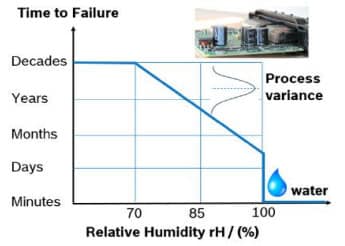
Also, intensive studies from BOSCH [2] confirm a similar situation, that exposure of assemblies to relative humidity higher the 70%rH and ionic activity of compounds in flux residues has a significant role in starting ECM.
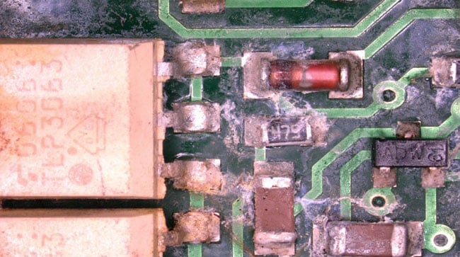
Additionally, the hard and brittle resin does not remain compact due to thermal mismatch and thermal cycling of all parts of the electronic assembly. Pictures from the field show the consequences of such thermal cycling after five years of operation. Exposure of this assembly by the chemical indicator of weak organic acid radicals showed an intensive blue discoloration. Such a result is evidence of active ionic compounds. When exposed to humidity and bias, such assembly is ready for ECM immediately.
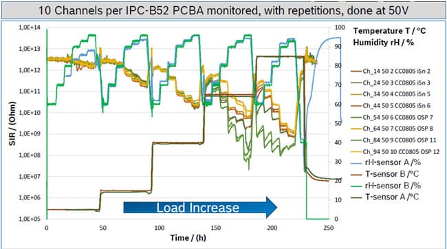
Surface insulation tests became the most significant for the qualification new assemblies in terms of robustness against EMC. However, standard SIR tests – 169 hrs/ 90%rH, 40°C- may no longer be a good tool. For higher voltages in assemblies in solar and automotive electronics (battery vehicles), the robustness against ECM must be confirmed even for a longer time and a harsher environment.

One example of such tests comes from automotive applications—the test with stepwise growing temperature and relative humidity.
It shows that areas at specific components cannot return to their initial surface resistance after several cycles of exposure to higher humidity and temperature. The reason is that even the well-composed no-clean flux released some ions after repeated exposure to a high moisture level.

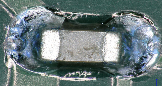
The following picture is a practical example of the consequences of high moisture (condensation) on the PCBA. The photo comes from repairing the control system of the heat pump for domestic heating. The device was installed inside the house in a room with moderate temperature and no significant temperature fluctuation. Nevertheless, the moisture condensation on the assembly surface during the rainy season caused dendrite growth. The place of installation was not in the tropic country but in the middle of Europe. PCB was not cleaned. Thus, the ionic residues activated the ECM.

In most cases, the damage of PCBA is not visible, but function can be disturbed. ECM causes not only dendrite growth but also leakage currents in the early stage. These unwanted currents can cause early exhaustion of batteries or shifting of some switching voltages.
Such leakage currents usually are not visible. Using Glass test boards, we can see the orientation of precipitates in the electrical field between the cathode and anode. The low current causes such orientation. For building a dendrite, there was not enough potential in the area. Technique by glass test board is optimal for studying such an effect because it is absolutely not destructive, and even the finest structures can be visible.


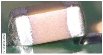
In picture 7. there is a capacitor from a sensor that should watch the presence of the textile fiber in the weaving machine. The atmospheric conditions inside the machine are 40°C, 65%rH. The sensors were found not reliable after some time. The reason was a capacitor and low surface insulation resistance around it. Visibly, there were no traces of any migration. However, the indicator of carboxylic groups has shown a presence of activators, which were not de-composed adequately during the soldering process. (not cleaned assembly).


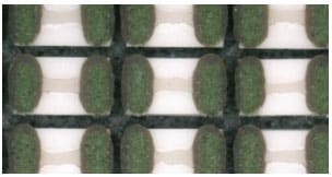
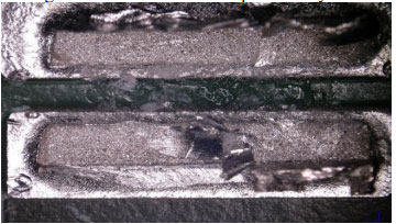
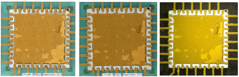
Cleaning of assemblies Building reliability against ECM by cleaning means that the assembly has no ionic active residues. The most critical places for disturbances of SIR are under the components and between terminals.
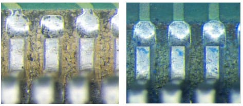
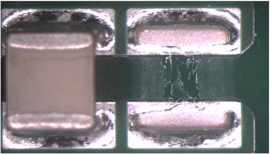
Due to limited mechanical cleaning action under components, some residues are often left there. In picture 7, we see two areas. So far, no dissolved flux residues – these might not be critical at the beginning of the lifetime of the assembly. Later, after breaking the flux layer by thermal shocks, it can cause ECM. The grayish areas, however, are dangerous immediately after such incomplete cleaning. These can be salts of organic acids and metal oxides produced during soldering. Also, it can be a less soluble part of the resin, forming a rough surface (therefore of a white color). In both cases, this is a risk for an assembly. Even non-ionic residues with a rough surface can attract moisture and move the critical rH for the assembly to lower values.
Cleaning of the Gap
The gap (the space between the package bottom and the substrate surface) is the most critical for cleaning today.
With the progress in design packages, the gap becomes thinner and larger. We can estimate the gap thickness from the thickness of the printed solder paste. The primary value is about 50% of a printed thickness (paste has approximately 50% volume of flux, which must leave the solder joint during soldering). Then, the terminal’s weight and shape decide the final thickness of the gap.


An adequately designed spray-cleaning machine must progress in cleaning the gap from both sides uniformly across the entire working space of the machine. Any inhomogeneity in the cleaning impact can cause prolonging of washing time (washing = first phase of cleaning (dissolving flux residues by the chemistry).
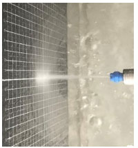
For spray-in-air cleaning technology, Direct Spray against the surface is the most effective way of agitation.
The spray beam brings the kinetic energy up to the surface, and streams of the liquid run from the hitting point to all sides along the board at the best angle to penetrate under components. All shadows due to tall components are suppressed with such an arrangement. Nozzle manifolds are scanning along the board.


Gap thickness has a prominent influence on the time necessary for cleaning. But not only the thickness is responsible for cleaning success. Also, the gap’s area and shape determine the cleaning time and challenge.
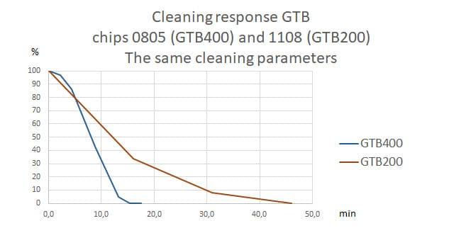
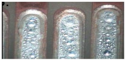
The following pictures demonstrate the effect of the narrow, long gap.


By using a short interval sequential cleaning technique (repeated short wash intervals, interruption + measuring of the result on automatic optical inspection), we found that the 2x longer gap needs a 3x longer time to a complete cleaning.

Often the gap size is reduced by the improper design of the board or even the component package.
A thicker solder mask than the pad is a bare-board manufacturing failure. It can cause too thick solder paste print, smeared print, and in extreme cases, tombstones. Thorough cleaning such a reduced gap under 10-5 um is impossible.
It is a standard design feature to draw a track under the component. If we like to optimize the cleaning process, we should avoid that!
Some passive components have so-called reverse geometry. Cleaning those always needs a longer time. Putting a track under such a component may make the cleaning even more difficult.


All these cases were only a short demonstration of the design and process failures, which compromise cleaning.
Cleaning assemblies with bottom terminated components (BTC)
BTC brings difficulties to the cleaning process. Cleaning results cannot be checked visually. Also, it is challenging to clean the small gap thickness and the large gap area thoroughly. But the most critical on the BTC is the different behavior of the flux residues during soldering. Leaded components and leaded SMT components have a pretty open surface of all solder joints. Fumes and gases from the flux can escape quickly and easily. Escaping gasses – degassing – from under BTC is never so fast because of obstacles in the form of IO´s at the package periphery (QFN) or a matrix of solder joints (LGA). Incomplete degassed flux is easy to recognize if you tore off the component. The residues are not hard but soft, sometimes sticky.
Incompletely degassed flux residues support the volatility of ions. Such an effect is visible in the result of the demonstration [4] – soldering the comb test board B24 as open and covered with the microscopic cover glass. (Fig. 19, 20,21). Measuring surface insulation resistance shows a significant drop of SIR on the covered solder joint area.


Flux residues under BTC can support the ECM more intensively than residues at other components with the open surface of solder joints. Therefore, the cleaning of BTC must be complete and thorough if we decide to clean.
But we cannot check cleaning results under BTC visually. Adjusting cleaning process parameters is, therefore, challenging. We have developed a tool for overcoming these difficulties. Glass test boards simulate BTC geometry. Additionally, such boards are built as test coupons for measuring the SIR. So it represents a tool for optical and electrochemical checking of an optimal cleaning result.
The first tests with such a tool discovered even more information than expected. We can monitor the changes in the flux residue structure and amount during the SIR test (due to higher temperatures during the test – 40°C). Possibly the degassing process can continue even during the test period. Also, we can easily measure the gap height under the component after soldering. The degassing process during soldering seems to lift the component due to bubbles unevenly. Often even large components like QFN with higher OI count sit not parallel with the board after soldering is finished. Such an uneven position can substantially influence the ability of the assembly to easy cleaning.

Cleaning BGA is much easier because of the high gap (about 200um). Also, the spaces between terminals (balls) are open from the beginning of the cleaning process. So, cleaning liquid flow under the component is not blocked.


Both components (QFN44 and FBGA1020) show an acceptable level of SIR after cleaning in our test. The minor solder residues under QFN 44 do not influence the SIR value. (after a 169hr test period).


As mentioned above, position and gap thickness substantially influence the cleaning result. When the component tilts during soldering, this represents an unpredictable change in the gap thickness. Especially components with a large heat lug in the center (QFN, QFN DR) have a big volume of flux to degas. These are very sensitive to a proper heat-lug print pattern design.
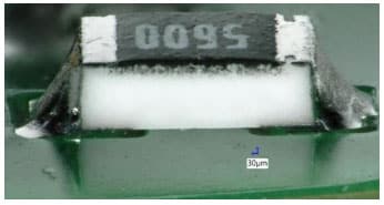
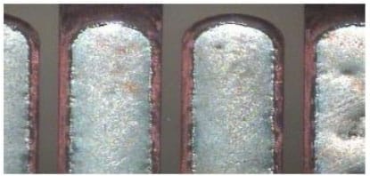
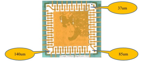
The following pictures show a sequence of cleaning progress under QFN DR124. Clearly, in one corner of the package, cleaning progresses very slowly. Gap thickness measuring shows that the critical corner has a gap thickness of only 37um, while the other corners have a much higher value.


Fig. 35. Cleaning progress of QFN DR124

Cleaning Process Control
The cleaning process for BTC is currently the most challenging part of the PCB assembly cleaning process. We need good stability and repeatability. The cleaning process shall be precisely controlled in all stages (wash, rinse, drying).
Commonly controlled parameters like time, temperature, cleaner concentration, and eventually conductivity of rinsing water are not enough to achieve satisfactory process stability. Usually, the other necessary analysis (like saturation and alkaline reserve of cleaning chemistry and organic residues in rinsing water) can be done only in the laboratory. Such an approach is slow and not suitable for higher production volumes.
We attempt to add such necessary sensors directly to the cleaning machine. The new Organic Carbon Sensor determines the right moment to refresh the active carbon filters on the water treatment plants on the cleaning system.
Tools like glass test boards are effective for fast proper parameter setting and pre-qualification studies, even in such productions where new assemblies are frequently coming into production.
Also, other factors substantially influence cleaning effectiveness besides process parameters and cleaning machine design innovations, which steadily come to the market.
These are design details on assembly (violation of fluid dynamic rules caused by improperly situated components) or package design details, which do not support easy cleaning.
A much close cooperation and knowledge transfer between component and assembly manufacturers are more than necessary. Optimization of sometimes tiny details may save a lot of time and cost and help to increase the reliability of final products.
Literature:
[1] Rajan Ambat, Ph.D. Sajjad Bahrebar Ph.D. (CELCORR, DTU)
Safe Operation Boundaries for PCBA under Climatic Conditions Based on Analysis of LC and ECM Data [SMTA Conference Amsterdam 2023]
[2].. Lothar Henneken Ph.D. (Robert Bosch GMBH)
Risk Prediction of Electrochemical Migration on Electronic Control Units – a Statistical Approach [SMTA Conference Amsterdam 2023]
[3] Ing. Vladimir Sitko, Dr. Mike Bixenmann ( PBT Works, Magnalytics) Optical Inspection and SIR Measuring under the Component Bodies using a SIR Glass Test Vehicle [Climatic Reliability Seminar DTU Cobenhaven 2023]
[4] Ms. Karen Tellefsen (Mac Dermid Alpha), Advanced SIR Testing For Trapped Solder Paste Flux Residue [SMTAI International 2020]