


")


LTCC (Low Temperature Co-fired Ceramic)
The use of LTCC material is gaining importance in applications in the field of communications. This is a multi-layer process used for the production of sophisticated HF components with good performance characteristics. The ceramic-based LTCC technology is an inexpensive substrate technology with which up to 50 layers are stacked on top of each other. The silver or gold conductor tracks are impressed on the “green” ceramic foil once the holes for the through contacts have been laser or mechanically generated. The various layers are then collected together and are pressed in a pressure chamber. Following lamination, the stack is sintered in a furnace, i.e. burned together at around +850 °C in process furnaces.
LTCC can be used to produce multi-layer modules in which cavities, Rs, Ls and Cs are integrated. Good thermal conductivity and a low TCE (Temperature Coefficient of Expansion) are achieved. The components are hermetically sealed, i.e. are stable against mechanical and thermal stress. The dielectric properties (er, tan d, the thickness) can be controlled very effectively.
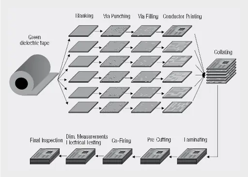
Fig. 2.93: LTCC production process
The main advantage of this technology is the high degree of miniaturisation and the ever-lower space requirement associated with it. This is illustrated by the following simple example. Rather than discreetly constructing a low-pass filter, there is the option of integrating the inductances and capacitances, e.g. as package type 0603. The integration is an important aspect in the field of RF applications.

Fig. 2.94: LTCC low-pass filter, package type 0603
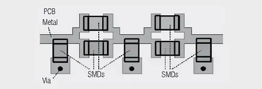
Fig. 2.95: Discreetly constructed low-pass filter
Low-pass filter
HF components based on LTCC technology are designed for use in various frequency bands from around 900 MHz to 6 GHz. Application areas for these components are, for example, Wireless LAN, Bluetooth®, HomeRF, GPS, PCS, GSM, DECT and PHS.
The high precision LTCC technology gives rise to low-loss RF components with reproducible, guaranteed properties and a low space requirement.
LPF low-pass filters for diverse applications are produced in the package types 0603 to 0805. The limit frequencies of these compact low-pass filters range form 900 MHz to 5.5 GHz. The insertion loss of the low-pass filter in the admission range is very low. The low-pass filters show comparably high attenuation in the blocked range.
Band-pass filter BPF
The smallest band-pass filter package type is 0805. A high level of attenuation is achieved over a very wide blocking range. The insertion loss in the admittance range is very low at approx. 2 dB, however somewhat higher than the insertion loss of low-pass filters.
The example of the band-pass filter for Bluetooth® serves to illustrate where attention should be paid in the selection of components.
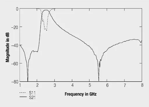
Fig. 2.96: Frequency response of the band-pass filter
To effectively suppress frequencies in the mobile phone range, the attenuation in the range from 900 MHz (GSM900) to 2.1 GHz should be as high as possible. The attenuation in the WLAN/HyperLAN range should also be high. For this reason, specific poles have been placed at these frequencies for the above filter.
Balun BAL
Symmetry transformers (baluns) with low insertion loss, as well as low amplitude and phase differences, can be achieved in LTCC technology. The asymmetrical (unbalanced) impedance is 50 Ω, the symmetrical (balanced) impedance can be 50 Ω, 100 Ω or 200 Ω. Two types of baluns are distinguished: LC type and Marchand type. In the case of the latter, no DC bias may be applied. It is recommended to connect a capacitor to ground in front of the pin where the DC voltage is input. Information on external circuitry and layout recommendations may be found in the datasheets.
Balun with integrated band-pass filter
A band-pass filter and a balun were integrated into a component to reduce the space requirement. Besides the high attenuation in the blocking range, low insertion loss is also achieved. The admission range of this newly developed component lies in the frequency range 2400–2500 MHz.
Numerous other components, such as diplexers, couplers and couplers with integrated low-pass filter or dual-band baluns, are available in this multi-layer technology.
Multilayer MCA
The MCA chip antennas based on LTCC technology stand out by virtue of their compact constructions and low weight and are suitable for applications in the fields of GPS, Bluetooth, 802.11b+g, UNII and 802.11a as well as for 868–960 MHz, also available as dual & triple band. In relation to their size, the antennas offer a large bandwidth and are easy to match. The input impedance is 50 Ω. The typical gain, depending on the antenna type, is around 1 dBi. The radiation properties of the antennas can be termed plane omnidirectional. Alignment charts are presented in the
datasheets.
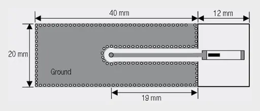
Fig. 2.97: Evaluation board for the antenna (example WE 748 891 0245)
The electrical parameters of the chip antennas are measured with test boards as shown in Figure 2.97. Many factors, e.g. the board type (dielectric constant) and the layout, affect the electrical properties of a chip antenna. The component values for the matching network shown in the datasheet cannot be assumed for this reason. These values only apply for the test boards used; they may however be used as starting values for determining the matching network in the application. The return loss can be significantly improved by matching the antenna.
To achieve the performance shown in the datasheet, it is important to ensure sufficient separation between the antenna and the ground plane. The antenna is preferably placed at a corner point of the board to avoid that the antenna is completely surrounded by a ground plane. Deviations from the suggested layout instructions can lead to changes in the alignment characteristics and input impedance. In general, care must be taken that the separation between the long side of the antenna and the ground plane is at least 5 mm. The separation between the antenna surface and the housing must be at least 1 mm.
The microstrip feed lead can be considered as part of the antenna system. It is recommended to connect the ground plane surrounding the input lead on the edges to the lower ground with through contacts. This serves to minimise the electric field on the edges and hence its influence on the antenna.
The efficiency η is the ratio between the radiant power and the input power. The efficiencies of the chip antennas derived from numerical calculation are presented in the following table. This includes antennas operating in the frequency range 2400–2500 MHz. Essential differences are the antenna dimensions and the gain. The standing wave ratio is a maximum of 2 for all antennas within the bandwidth.
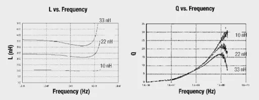
Air coil KI; RFH; RFI
The classic inductor is a configuration of one or more wire windings on a magnetically non-conducting coil former. In contrast to coils with magnetic coil formers or cores, this component‘s advantage is in its current independent inductance and the fact that it shows no saturation effect.
Further very important advantages are the linear impedance over a wide frequency range, i.e.

and a very high quality factor Q (typ. 50–100). The following relationship exists for an inductance L and the winding turns n:
![]()
The air coil has a parasitic capacitance dependent on winding diameter, wire thickness as well as layer and winding structure, which mainly exists between neighboring windings (Figure 2.98), but for SMD components also occurs between both the connection pads.
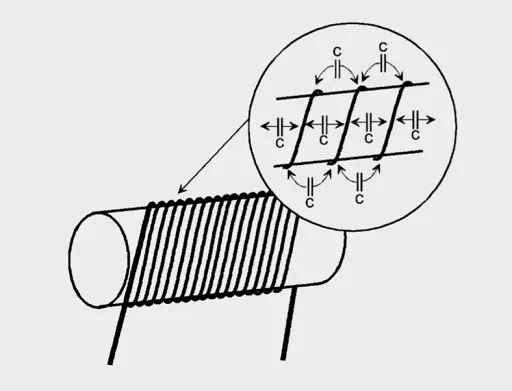
Fig. 2.98: Schematic representation of parasitic capacitance between coil windings
The self-resonant frequency, above which the component shows capacitive characteristics, results from the inductance and the parasitic capacitance.
The series of KI ceramic SMD inductors are examples of air coils (Figure 2.99).
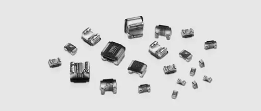
Fig. 2.99: Example of ceramic SMD inductors
The solder pads on the coil former are designed to be very small (Figure 2.100), in order that the inductors achieve a high self-resonant frequency.
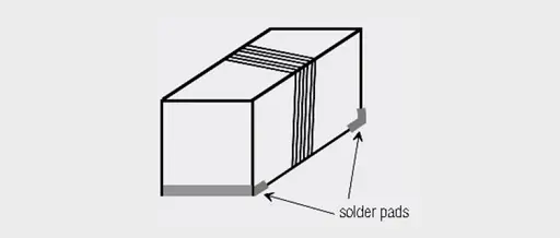
Fig. 2.100: Schematic construction of a ceramic inductor
Self-resonant frequencies of well above 10 GHz are thus attained.
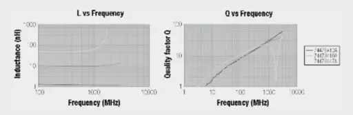
The RFH series is available if higher current carrying capacities are required. The components are wound on ceramic or ferrite cores depending on the inductance value.
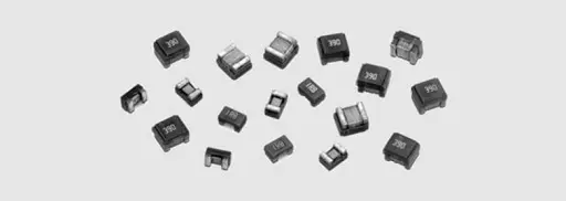
Fig. 2.101: Ferrit SMD Inductor RFH
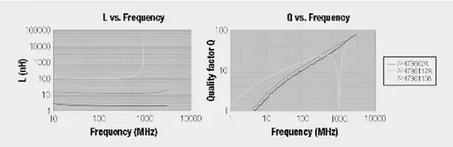
The range of wound RF inductors is rounded off with the RFI series. The components wound on ferrite stand out by virtue of their very high inductance values in relation to their package size.
RF Multilayer Ceramic Inductor MK
The construction of an SMD inductor (Figure 2.102) MK differs from that of a conventional air coil in that the “coil” is printed on a ceramic substrate. This presents the following advantages:
- Very low inductances achievable
- Very low parasitic capacitance and therefore high resonant frequency
- Relatively high current carrying capacity of typ. 300 mA

Fig. 2.102: MK multilayer ceramic SMD inductor
The specifications of various multilayer ceramic SMD inductors are shown in Figure 2.103.
Type 0201:
Type 0402:
Type 0603:
The preferred field of application of these components lies in the high- frequency range, in filter circuits and oscillator circuits.
ABC of CLR: Chapter L Inductors
RF Components
EPCI licensed content by: Würth Elektronik eiSos, Trilogy of Magnetics, handbook printouts can be ordered here.

This page content is licensed under a Creative Commons Attribution-Share Alike 4.0 International License.


Discussion about this post