


")


C1.1 CAPACITANCE
The Capacitance is determined by, among other things, the characteristics of the dielectric material. International standards speak of the Dielectric Constant or permittivity, designated by the symbol ε.
C1.1.1 Description
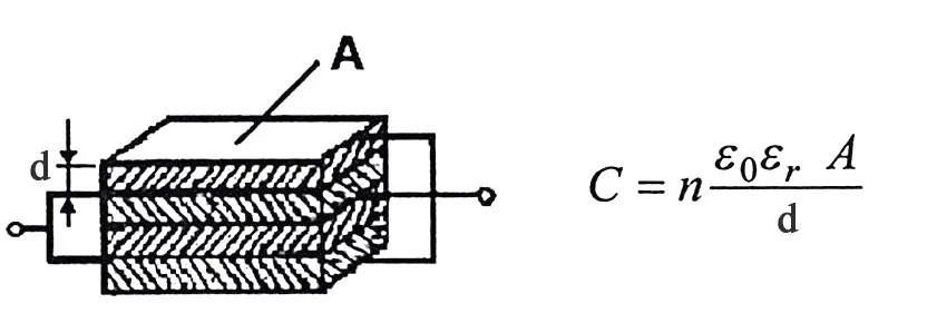
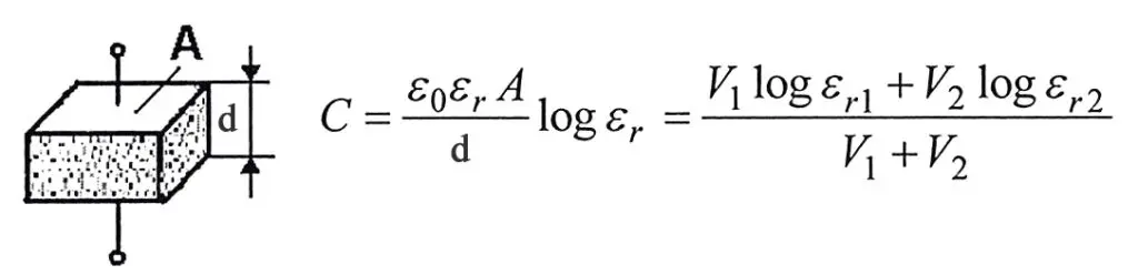
A capacitor serves as a reservoir for electric charges. The size of the ”reservoir” is called capacitance and is expressed in the quantity F(arad) or As/V. The principle Figure C1-1 shows how the capacitance is directly proportional to the active area A and to the dielectric constant and inversely proportional to the distance between the electrodes. The formula in the figure is applicable to vacuum and air.
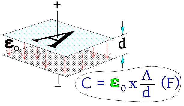
A = area (m2),
d = distance between electrodes (m),
ε0 = dielectric constant for vacuum (≈air) = 1×10⁻⁹/36π.
Figure C1-1. The principle of capacitance, C.
If the electric charge quantity of the capacitor is designated with Q (As), then the general formula C1-1 is valid.
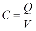 ……………………………… [C1-1]
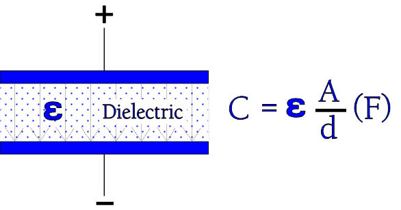 Figure C1-2. Dielectric with its constant .
If we now insert an insulator material between the electrodes as shown in Figure C3-2, the formula in the figures C3-1 and -2 get the following general expression
 ………………………………. [C1-2]
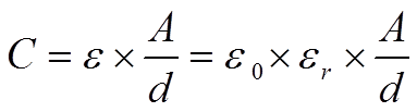
εr is a relative number – the relative dielectric constant – which tells us how many times the capacitance is magnified when we exchange the air gap between the electrodes with different dielectric materials. That’s the relative dielectric constant εr which is given in technical tables and catalogues. Table below shows dielectric constant of the most common materials.
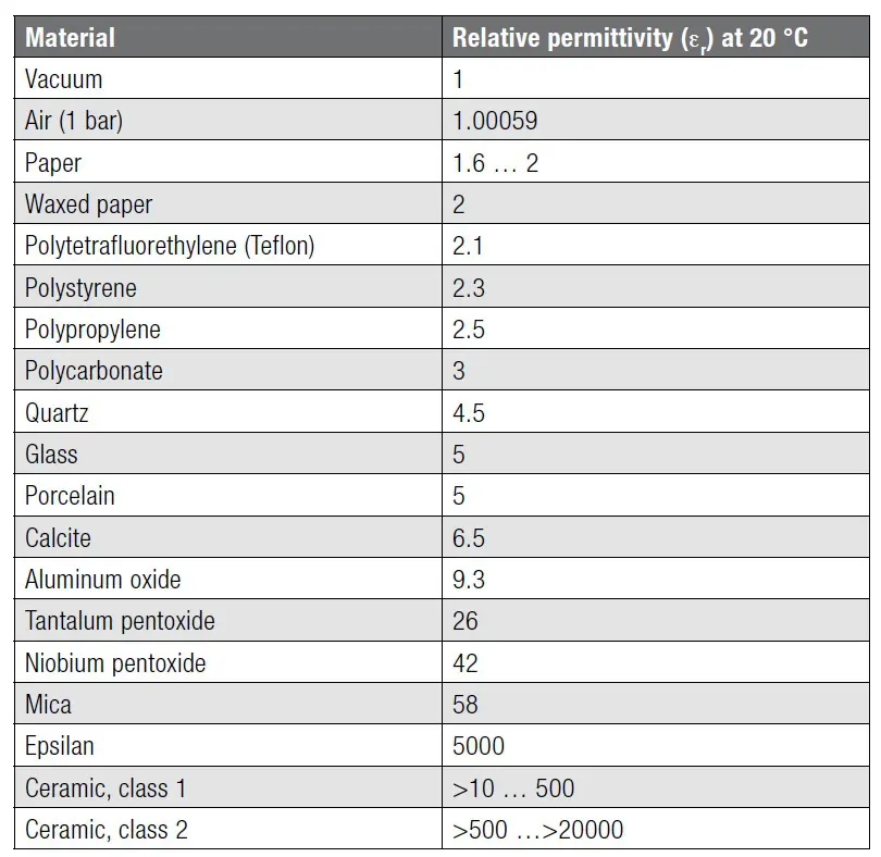
Figure C1-2b Dielectric constants of most common insulating materials
Capacitive Reactance
If we change polarity in Figure C1-2 by applying an AC voltage over the capacitor, it will cause a certain resistance in the circuit, a so called capacitive reactance, XC, expressed in ohms.
The reactance is inversely proportional to frequency according to the formula

…………………….. [C1-3]
- ω = 2 x π x f,
- f = frequency in Hz,
- C = capacitance in F.
Measure of miniaturization
The desired miniaturization of different capacitor types can be expressed in different ways. The smallest rated voltage for electrostatic capacitors often is more than enough for the application as shown in section C2.1.4 also. Hence we usually disregard the voltage and compare the various types by means of their maximum possible C/V rate which means capacitance C per unit volume V (d * A in the Figure C1-1).
According to the Formula C1-2 we get C/V = ε0 * εr * A/(d * A * d) = ε0 * εr /d2.
The rate C/V will be at maximum for dmin, i.e., for VRmin.
In electrolytic capacitors the rated voltage plays a greater role because it can be adopted also to very low working voltages. Here the capacitors are grouped according to their charge quantity, that is to CR*VR. We refer to the CV product.
Connections
If we connect capacitors in parallel as shown in Figure C1-3 the active area (and hence the capacitance) increases with all additional capacitor elements.
 Figure C1-3. Principle figure of the total capacitance when the elements are connected in parallel.
Formula for the total capacitance of connections in parallel:
![]() ……………. [C1-4]
……………. [C1-4]
Figure C1-4 shows in principle how connection in series increases the dielectric thickness without changing the charge quantity. The capacitance decreases proportionally to the increase of dielectric thickness.
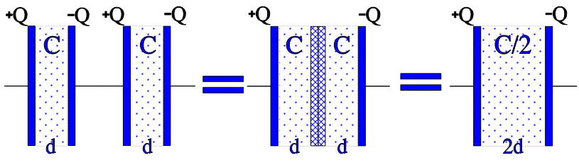 Figure C1-4. The principle of series connection.
The figure shows a simplified picture of series connection with two equally large part capacitors. If we instead choose capacitor elements of unequal size the charge quantities on the different electrodes still will be equally large, i.e. Q = CV = C1V1 = C2V2 = C3V3; Q/C = V; Q/C1 = V1; Q/C2 = V2; Q/C3 = V3…But V1 + V2 + V3 +….= V. This gives us in general the total capacitance for
Series connection:
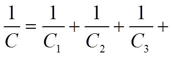 ………….[C1-5]
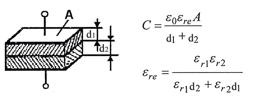
Mixed dielectrics
So called mixed dielectrics have become more and more common. They consist of different film materials in the same capacitor. For example by winding a capacitor with both a paper and a polyester film dielectric we combine the excellent self healing properties of paper and the relatively high insulation resistance of polyester. In principle it’s still a question of two capacitor elements in series connection, with the same area and the dielectric thickness d1 + d2. Then the relation we depicted above is valid: Q = VC = V1C1 = V2C2; V1 x ε1 x A/d1 = V2 x ε2 x A/d2; if we denounce the electric field intensity E we then obtain
ε1 x E1 = ε2 x E2, or in general
ε1 x E1 = ε2 x E2 = ε3 x E3 = ……………………… [C1-6]
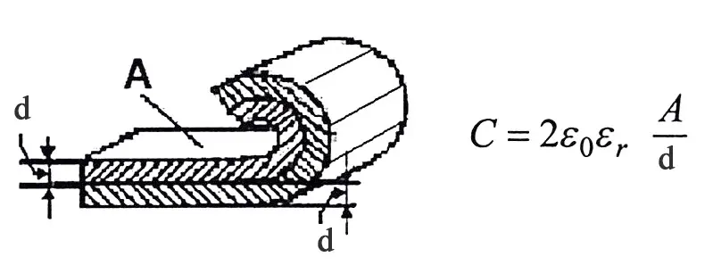
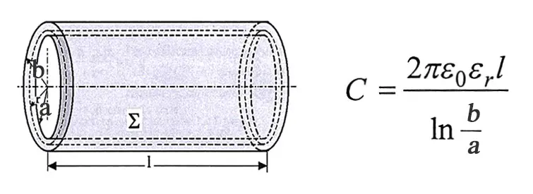
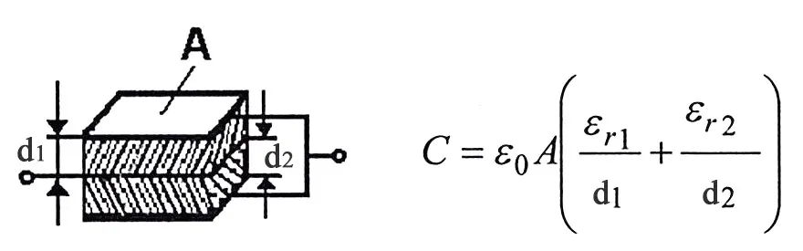
Other non-plate and various geometry capacitance calculations
The capacitance calculation by equation [C1-2] and illustrated in figure C1-2 are based on plane capacitor type. However, there are many other capacitor construction types and geometries on the market. See the theoretical capacitance value calculation for some of other geometries as well as mixed dielectric situations below:
Capacitance standardized values and tolerance
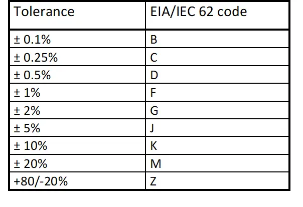
Following international standards EIA/IEC 62, capacitance values and tolerances are standardized as follows:
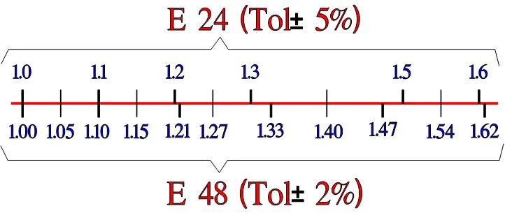
E range
Capacitance is following standardized “E ranges” defined per logarithmic-steps such as E3, E6 … E24, E48 steps.
Naturally, the selected E-range is also linked to the tolerance field – not to overlap between the next capacitance tolerance range – see bellow.
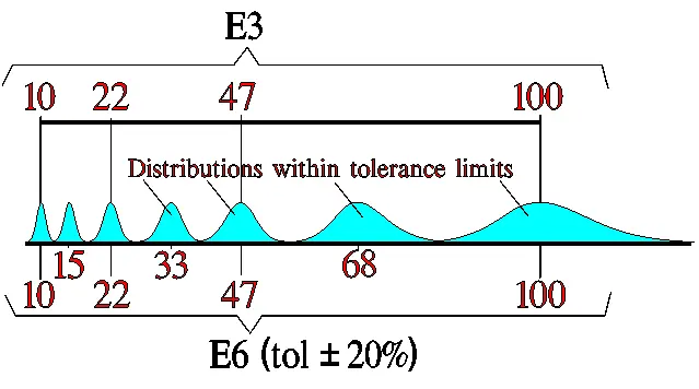
Specific capacitor technologies’ E range is driven by its capability to produce reproducible and tight tolerance capacitance value in mass production. You can find the relevant capacitance values and tolerance ranges defined in manufacturers’ catalogues.
C 1.1.2 Dipoles
The section about dipoles and of dielectric absorption is of vital importance for the understanding of the practical capacitor. All materials contain some kind of dipoles, i.e. electrically polar elements. When they are subjected to an electric field it creates a torsional moment which, depending on the field strength, will tend to align them in this field. These torsional moments can be divided into four groups. Those which are caused by
- electron movements in atoms and molecules,
- atom movements in symmetrical molecules,
- atom movements in unsymmetrical molecules and
- charge accumulations on interfaces between different materials in the dielectric.
As long as the capacitor is not biased, the dipoles have a random orientation, without any resulting pole. It may in principle looks like the Figure C1-5.
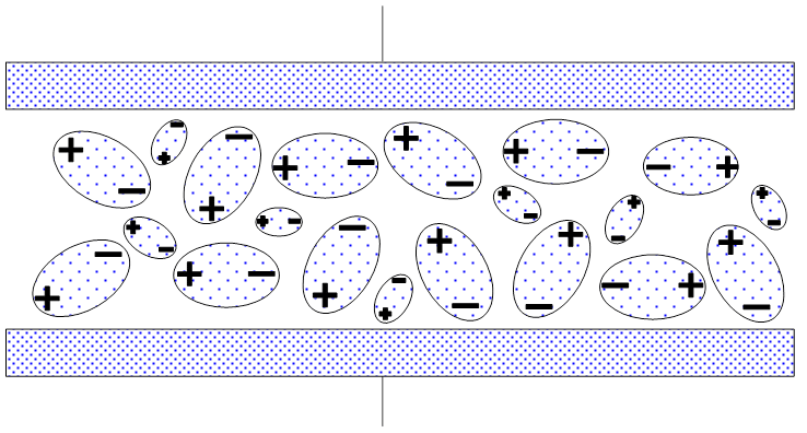
Figure C1-5. Dipole orientation in an unbiased dielectric.
If they should be subjected to an electric field strength as in Figure C1-6 they will after a specific time tend to be aligned in dipole chains. The dielectric material has been polarized.

Figure C1-6. Perfectly-aligned dipole chains.
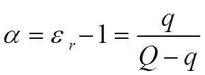
The electric field strength (the number of imaginary field lines which would have formed in vacuum) has been reduced with the number of established dipole chains. Every dipole chain binds in the interface towards for example the positive electrode a + charge and the number of free charge carriers in the electrode has been reduced to a corresponding degree. Thus, after the alignment time of the dipoles, the electrode is able to receive as many new free charge carriers as those the dipole chains have bound without creating an increase of the electric field strength (or the voltage) above that of the starting point. This means a corresponding increase in capacitance. If we call this polarizability , the number of bound charges q and the number of charges at the starting point Q, it can be shown that
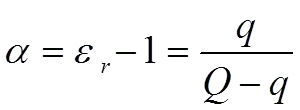
……………………. [C1-7]
The function of a versus frequency is shown in Figure C1-8 below.
Because r depending on dielectric material varies approximately between two and many thousands we realize what an enormous significance the material dipoles and the polarizability plays.
Frequency dependence of capacitance
The velocity with which a dipole react for an applied electric field is called its relaxation time. These relaxation times range from 10-17 s for the electron dependent dipoles to several hours for the large molecular complexes. That means that the fastest dipoles keep up with all practical frequencies while the slower to a varying degree need time to contribute with capacitance-increasing dipole chains. The phenomenon can be described as a basic capacitor combined with a number of additional capacitor elements hidden in resistive circuits with shorter or longer time constants (Figure C1-7).
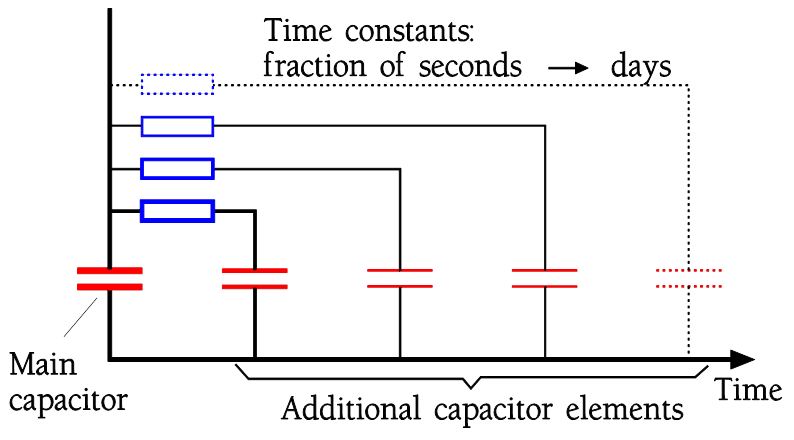
Figure C1-7. Dipole categories in a capacitor.
An example of the frequency range that different types of dipoles contribute to is shown in Figure C1-8.
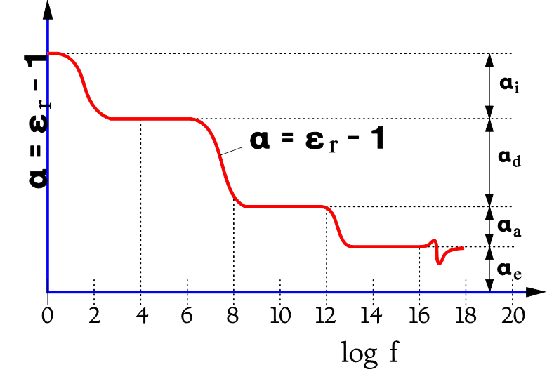
- αe = dipole effect from electron movements;
- αa = dipole effect from atom movements in symmetrical dipoles;
- αd = dipole effect from atom movements in unsymmetrical molecules;
- αi = interface dependent dipoles.
Figure C1-8. Typical example of schematic variance of polarizability in a solid material with frequency.
Thus, the capacitance decreases with increasing frequency. In components with large dielectric losses and a considerable percentage of inert dipoles we will learn how the impedance curve starts deviating from the nominal capacitive reactance curve when we approach the resonance frequency. Figure C1-20.
C 1.1.3 Dielectric absorption
If the dipoles have been ”activated” to form a dipole chain it will take a corresponding time to “deactivate” them at the same temperature. In Figure C1-9 it is presupposed that the capacitor first has been charged, then momentarily short circuited and finally left open. Those dipole chains which were too inert to react during the short circuiting moment kept their charges captured in the electrode. After a while in the absence of an electric field they begin to assume random, unaligned positions, releasing the captured charges in the electrodes (Figure C1-9). The released charges are manifested as a residual voltage in the capacitor and is measured in V. This residual voltage is a measure on the dielectric absorption ”DA” of the capacitor and is expressed in percent of the initial voltage applied.
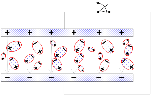
Figure C1-9. Effect of dielectric absorption.
DA is generally an unwanted property which burdens certain dielectric materials severely, others little or quite negligibly. It may sometimes cause problems we will discuss later.
The determination of DA is made by biasing the capacitor with a DC voltage for a certain period of time, then short circuiting the part over a resistor for a specified number of seconds and finally leaving it open for a number of minutes before the residual voltage is read. It is expressed in percent of the charging voltage. Voltages, times and resistances are specified in different standards which sometimes differ. Examples of how the times influence the results are shown in Table C3-1 where the records are done at 25 °C. DA increases strongly with rising temperature.
Table C1-1. Examples of DA @ 25°C
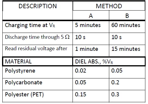
Knowledge of the dielectric absorption of capacitors is often vital for optimum circuit design. Thus we will provide DA values in the part summaries following every material group. Primarily, the values are obtained based on procedures the same as or equal to either of the methods in Table C1-1 above.
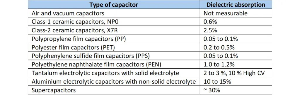
See below table of the most common capacitor technologies’ dielectric absorption:
ABC of CLR: Chapter C Capacitors
EPCI licenced content by:
[1] EPCI European Passive Components Institute experts original articles
[2] CLR Passive Components Handbook by P-O.Fagerholt*
*used under EPCI copyright from CTI Corporation, USA

This page content is licensed under a Creative Commons Attribution-ShareAlike 4.0 International License.


