


")


This paper will present a novel technology (CNF-MIM) combining Carbon Nanofiber (CNF) materials and MIM (metal-insulator-metal)-like technology, enabling capacitors with total thickness lower than 40 µm suitable for use in future miniaturized electronics.
The paper was presented by Maria Bylund, Smoltek AB, Gothenburg, Sweden at the 3rd PCNS 7-10th September 2021, Milano, Italy as paper No.5.3. and voted by attendees as:
BEST PAPER AWARD
The ultra-thin and discrete CNF-MIM capacitors have been manufactured and characterized on several substrates, showing excellent electrical properties such as high capacitance density of several hundreds of nF/mm2, ESR (equivalent series resistance) in the mOhm range, low ESL (equivalent series inductance) on the order of 10 pH thus being promising for a multitude of applications within the semiconductor industry. To assess the long-term durability, CNF-MIM capacitors have also been subjected to prolonged exposure to high temperature and constant voltage bias environments following a HTS (high temperature storage) and BTS (biased temperature stress) standard. The CNF-MIM capacitor show initial robustness against degradation in these scenarios.
INTRODUCTION
The Internet of Things (IoT) is constantly evolving, creating new solutions and merging products and functions to new smart devices integrating more and more functions into a single product. The desire to have high performance products that are thin and low weight creates a demand for miniaturization and pushing the need for integrating more devices onto a single chip. Then space becomes a valuable commodity inside the products and thereby the need for innovative solutions for System in Package (SiP) and System on Chip (SoC) schemes by mounting them on interposers and in 3D stacking. This leads to more components being integrated in the same space. One way to facilitate this is to decrease the size of the components, while maintaining or improving the performance, thereby fulfilling Moore’s law [1]. Here, high capacitance density, low profile height capacitors with small footprint area can be implemented, shortening the leads, and coming close to active components for noise suppression and decoupling applications [2], [3]
The demand on current and future applications in e.g., 5G, IoT, automotive industry and mining is that components are reliable under different ambient conditions such as prolonged heating. Reliability in performance of every single component is vital, it must not degrade or change properties or fail with temperature or voltage change. Degradation or even failure of components can occur when subjected to heating which can give a drift in electrical characteristics which will affect performance, not only of the component itself, but also of the entire system where it is used.
For capacitors, behavior such as decreased capacitance and breakdown voltage, increased leakage current and equivalent series resistance (ESR) are common signs of degradation of properties. Ideally, the capacitance density should remain the same regardless of changes in temperature or voltage biasing. In the ideal case, fully integrated capacitors on a chip are fabricated in fully CMOS compatible processes hence setting restrictions for which materials can be used and the temperature at which they are manufactured.
Widely used in the market today are Multi Layered Ceramic Capacitors (MLCC) providing high capacitance density and low ESR. The profile height for the MLCC is on the order of hundreds of microns. However, the sintering process requires high temperatures for the ceramic insulator which means it is not suitable for the CMOS process chain and therefore it can only be used as a discrete component.
An alternative way to increase the available surface area, by as much as 25-30 times, is to etch pores in the substrate itself and there realize the capacitor. However, to create the pores the substrates need to be thicker, at least 80 µm, and the time-consuming etching process might mechanically weaken the device [4], [5]. By etching pores as deep as 200 µm, a capacitance density of 1 µF/mm2 has been demonstrated [6].
To enhance the surface of the electrodes in the miniature MIM configuration, Vertically Aligned Carbon Nano Fibers (VACNFs) can be used, thereby creating a CNF-MIM capacitors which have shown a progressively increasing capacitance density [7] – [9]. The latest presented value being 650 nF/mm2 for a total profile height of 7 µm [10] as well as a small footprint for decoupling, filtering, and noise suppression purposes. The CNF-MIM has shown stability of the capacitance density against voltage and temperature variations, and they conform well to X7R standard ratings [11]. The CNF-MIM has also been realized on different substrates such as silicon, alumina, and glass [12].
In this work, we present studies of the electrical behavior at high temperature and biasing voltage of the CNF-based capacitors that have been fabricated in a CMOS compatible process. Characterization of the devices’ performance in terms of capacitance density, ESR, Equivalent Series Inductance (ESL) and leakage current was performed.
Capacitor fabrication
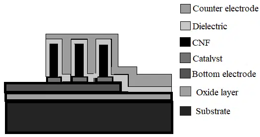
The making of a CNF-MIM starts with a high-resistivity silicon substrate, covered with an insulating layer of silicon oxide, where the bottom electrode is formed using a Ti/Cu metal stack. The catalyst is deposited using physical vapor deposition, PVD on lithographically defined pattern. VACNFs are then grown on the bottom electrode using plasma-enhanced chemical vapor deposition (PECVD). The dielectric is deposited on the fibers using conformal coating, i.e., atomic layer deposition (ALD) technique. By choosing different dielectric materials and layer thickness, it is possible to tailor the electrical properties such as capacitance density and breakdown voltage to better suit the application where the finished capacitor will be used. Using ALD, a thin layer of TiN is deposited as a counter electrode, followed by the deposition of Ti/Al by sputtering. A cross-section of a competed device is shown in Fig.1.
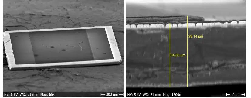
Ultra-thin devices are manufactured the same way as the standard devices, only they are manufactured on a silicon-on-oxide (SOI) wafer, and are, after manufacturing is complete, thinned down by removing the so-called handle layer using a high density inductive coupled plasma reactive ion etching (ICP RIE) process giving a thickness of less than 40 µm, see Fig. 2.
Characterization of devices
Scanning electron microscopy (SEM) is used to characterize the fibers after growth. Fig.2 shows a SEM image of CNFs at 40 degrees tilt. SEM is also used to get an approximation of the fiber length since this will give an estimation of the capacitance density of the finished device. The electrical characterization of the capacitors is obtained using a low frequency vector network analyzer (VNA) for S-parameter measurements ranging from 10 Hz to 3 GHz. Prior to measuring, a standard SOLT (Short-Open-Load-Through) calibration is performed to ensure a correct and accurate characterization. Data from the measurements are used to calculate capacitance at frequencies well below the self-resonance frequency (SRF) and the impedance characteristics of the device. These can be derived directly from the S-parameters matrix. Extraction of the equivalent series resistance (ESR) is made at the self-resonance frequency SRF and the equivalent series inductance (ESL) comes from the slope of the imaginary part of the impedance at frequencies above SRF. Dielectric properties, such as leakage current and breakdown voltage are measured using a Keithley 4200SCS Parameter Analyzer.
Reliability experiments
Two sets of experiments were set up to attain long-term reliability data for the CNF-MIMs. First, the devices were placed in an oven at a temperature of 85 degrees Celsius, where they stayed for 1200 hours. Secondly, the devices were mounted on a custom-made printed circuit board (PCB) using conducting epoxy and then bonded using a deep trench 25 µm gold wire bonding machine. Then the devices were biased with 1 V, and again placed in the oven at the elevated temperature of 85 degrees Celsius for a period of 1000 hours. The PCB enables the simultaneous biasing of eight devices at the same time.
For the first part of the reliability test, the devices were scanned with regards to both RF and DC in the previously mentioned Keithley 4200 SCS parameter analyzer and a Keysight E5061B low frequency VNA. The devices were screened before, periodically during and finally after to evaluate the possibility of degradation of device characteristics. For the second part of the reliability test, the devices were screened before and after the completion of the test time.
The thinned-down devices were characterized with regards to RF and DC before and after thinning down to make sure that the function of the devices is not lost in the processing.
RESULTS AND DISCUSSION
Reliability tests
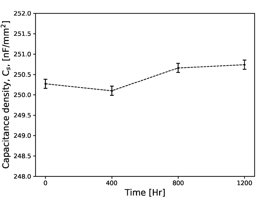
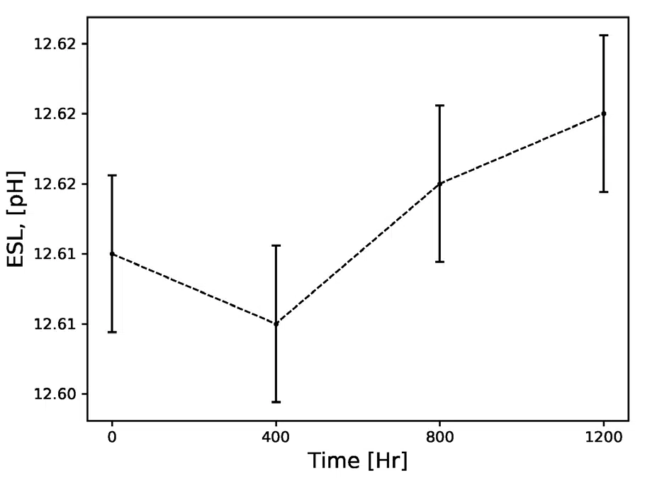
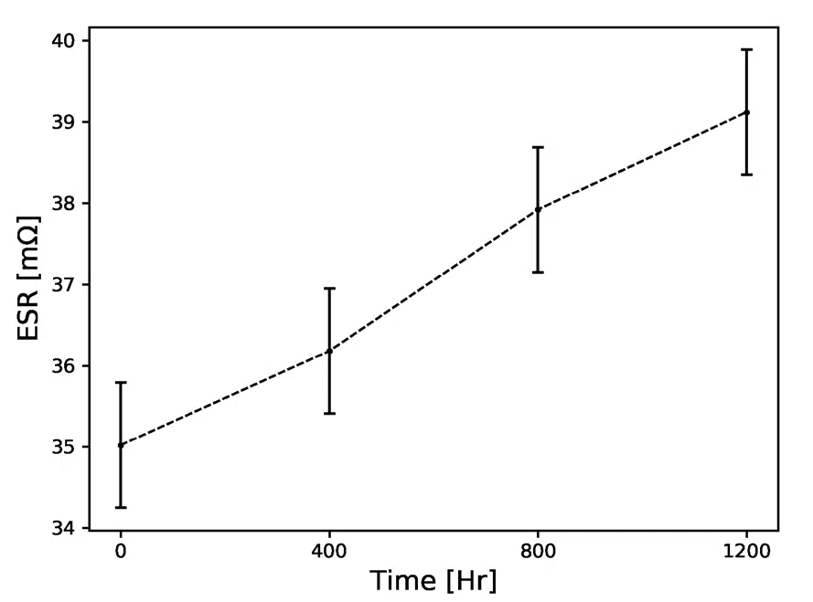
Results will be presented with a focus on how well the CNF-MIM device maintain the properties and characteristics. The first test, high temperature storage (HTS) was to expose the devices to an elevated temperature of 85 degrees Celsius for 1200 hours, and the devices were screened before, during and after the experiment. Prior to the test, the capacitance density was found to be approximately 250 nF/mm2 with an ESR of around 50 mOhm and an ESL of 10-15 pH. To detect any possible degradation of the devices, they were periodically screened, and it was found that the capacitance density and ESL remained practically unchanged for the entire period of time. See Fig. 2.
Devices used for the biased temperature stress (BTS) test, showed a capacitance density of approximately 400 nF/mm2, an ESR of 200 mOhm and an ESL of 10 pH. The isolation resistance of these devices was found to be in the order of 10-30 GOhm. These devices were not screened during the test time. After 1000 hours had passed, the devices were removed from the high-temperature environment and remeasured. Similar to the unbiased samples it was seen that regarding the capacitance density and ESL, the devices are largely unaffected by this experiment.
However, for both sets of devices, the ESR degraded by 10-20 %. For the HTS set, ESR before was 50 mOH and after 55-60 mOhm and for the BTS, that started at 200 mOhm it was 220-250 mOhm after. Some of the degradation can, most likely, be traced back to the fact that the probing surface degrades from repeated probing.
Regarding the isolation resistance over time, the results are inconclusive. The IR was seen to change both in negative and positive direction. However, all devices remained in the GOhm range. This feature will need further investigation.
Ultra-thin devices
After manufacturing, the ultra-thin devices were characterized in RF and DC performance. The capacitance density was found to be 500 nF/mm2, with an ESR of 7 mOhm and ESL of 14.74 pH. When the devices had been thinned down, they were remeasured, and it was found to be approximately the same, which means that the thinned-down devices have a comparable performance to the standard CNF-MIM while having a profile height of slightly less than 40 µm, including a substrate.
Other substrates for CNF-MIM
It is also possible to manufacture the CNF-MIM on other substrates than silicon. The CNF-MIM has been realized on different substrates such as alumina and glass where they show the same performance as the standard CNF-MIM on silicon.

CONCLUSION
We presented a MIM capacitor with VACNFs that creates a 3D structure which increases the available surface and, hence, increase the capacitance of the device. The CNF-MIM was subjected to reliability testing at an elevated temperature with or without constant biasing for a prolonged time. The intrinsic properties such as capacitance density, ESR, ESL and isolation resistance were monitored and evaluated. It was found that capacitance density and ESL remained roughly the same for both biased and unbiased testing. The ESR increased by 10-20 % but that could be explained to be related to degradation from repeated probing on the pads. Isolation resistance remained high during the entire test period.
Ultra-thin devices with a total device height, including a substrate, of slightly less than 40 µm was realized and compared to the standard CNF-MIM and found to perform equally well regarding properties and performance.
This highly adaptable device, showing high capacitance density, low ESR, low ESL and high isolation resistance and at the same time being the thinnest capacitor in the world makes it a strong competitor when compared to other devices found on the market. Even if the VACNFs add to the total height of the finished device, the height is only a fraction of comparable commercial off-the-shelf devices thus, making it a true competitor for future use in miniaturization and smart packaging solutions. It is highly reliable when subjected to elevated temperatures for prolonged periods of time. The CNF-MIM can also be realized on different substrates such as alumina and glass.
REFERENCES
[1] G. E. Moore, “Cramming More Components onto Integrated Circuits,” Electronics, vol. 38, no. 8, Apr. 1965, W. Chen, W.R. Bottoms, “Heterogeneous integration Roadmap”, International Conference on Electronics Packaging (ICEP), 2017, pp. 302-305, doi: 10.23919/ICEP.2017.7939380
[2] M. Popovich, M. Sotman, A. Kolodny and E. G. Friedman, “Effective Radii of On-Chip Decoupling Capacitors,” IEEE Transactions on Very Large Scale Integration (VLSI) Systems, vol. 16, no. 7, pp. 894-907, 2008. [2] J. Chen and L. He, “Noise driven in-package decoupling capacitor optimization for power integrity,” in Proceedings of the 2006 international symposium on Physical design, San Jose, 2006
[3] M. M. Waldrop, “The chips are down for Moore’s law,” Nature, vol. 530, no. 7589, Feb. 2016, p. 144, doi:10.1038/530144a.
[4] C. Bunel, “ipdia – The 3D Silicon Leader,” in Int. Symposiµm on 3D Power Electronics Integration and Manufacturing, Raleigh, USA, 2016. [4] C. Bunel et al., “Low profile integrated passive devices with 3D high density capacitors ideal for embedded and die stacking solutions,” in 4th Electronic System-Integration Technology Conference, Sep 2012,2012. [5] L. Strambini et al., “Three-dimensional silicon-integrated capacitor with unprecedented areal capacitance for on-chip energy storage,” Nano Energy, vol. 68, p. 104281, 2020.
[5] H. Hu, S. Harb, N. Kutkut, I. Batarseh, and Z. J. Shen, “A Review of Power Decoupling Techniques for Microinverters With Three Different Decoupling Capacitor Locations in PV Systems,” IEEE Transactions on Power Electronics, vol. 28, no. 6, Jun. 20 [1]13, pp. 2711–2726, doi:10.1109/TPEL.2012.2221482.
[6] M. Popovich, M. Sotman, A. Kolodny, and E. G. Friedman, “Effective Radii of On-Chip Decoupling Capacitors,” IEEE Transactions on Very Large-Scale Integration (VLSI) Systems, vol. 16, no. 7, Jul. 2008, pp. 894–907, doi:10.1109/TVLSI.2008.2000454.
[7] A. M. Saleem, R. Andersson, V. Desmaris and P. Enoksson, “Integrated on-chip solid state capacitor based on vertically aligned carbon nanofibers, grown using a CMOS temperature compatible process,” Solid-State Electronics, vol. 139, pp. 75 – 79, 2018. [7] R. Andersson, A. M. Saleem and V. Desmaris, “Integrated Fully Solid[1]State Capacitor Based on Carbon Nanofibers and Dielectrics,” in 2018 IEEE 68th Electronic Components and Technology Conference (ECTC), 2018. [8] A. M. Saleem, R. Andersson, M. Bylund, C. Goemare, G. Pacot, M. S. Kabir and V. Desmaris, “Fully Solid-State Integrated Capacitors Based on Carbon Nanofibers and Dielectrics with Specific Capacitances Higher Than 200 nF/mm2,” in 2019 IEEE 69th Electronic Components and Technology Conference (ECTC), 2019.
[8] A. M. Saleem, R. Andersson, V. Desmaris, and P. Enoksson, “Integrated on-chip solid state capacitor based on vertically aligned carbon nanofibers, grown using a CMOS temperature compatible process,” Solid-State Electronics, vol. 139, Jan. 2018, pp. 75–79, doi:10.1016/j.sse.2017.10.037.
[9] R. Andersson, A. M. Saleem and V. Desmaris, “Integrated fully solid-state capacitor based on carbon nanofibers and dielectrics,” Proc. 2018 IEEE 68th Electronic Components and Technology (ECTC), 2018, pp. 2307-2312, doi: 10.1109/ECTC.2018.00348.
[10] S. Krause, A. Rickard, M. Bylund, A. M. Saleem, M. Kabir and V. Desmaris, “Ultra-thin capacitors based on carbon nanofibers with ultra-high capacitance density,” in The IEEE Electrical Design of Advanced Packaging and Systems (EDAPS), Kaohsiung, 2019.
[11] M. Bylund et al., ”Robustness of carbon nanofiber-based MIM capacitors with ultra-high capacitance density to electrical and thermal stress”, in IEEE 68th Electronic Components and Technology Conference, 2020
[12] R. Andersson et al., “Electrical performance and robustness of ultrathin high-density carbon nanofibers capacitors on silicon, alumina and glass substrate materials,” International Symposium on Microelectronics, vol. 2020, no.1, pp. 000206-000210, Sept. 2020.


