


")


Increase of capacitors’ energy density is of prime interest in number of today’s applications. High energy density, high voltage capacitors are especially needed in fast-growing segments such as automotive, renewable energy generation and transmission, medical etc. This paper evaluates high energy density low Curie ceramic dielectric materials. The paper was presented by Tomas Zednicek, EPCI, Czech Republic at the 3rd PCNS 7-10th September 2021, Milano, Italy as paper No.1.2.
1. ABSTRACT
Film power capacitors are dominating the high voltage segment; however, this technology is limited with lifetime at high temperatures and relatively low energy density level. High capacitance, high energy density MLCC capacitors based on class II dielectric materials offer small, compact size, high reliability, and high temperature range, however it shows significant capacitance (and energy) deterioration with applied voltage that reduces its real energy storage capability as its remarkable disadvantage.
This paper presents a study on suitability of doped BaTiO3 (BT) based, ferroelectric ceramic materials BCST and BT-11BS with low Curie temperatures as high energy density capacitor dielectrics. Aim of the research was to evaluate key features of these materials and optimize its process parameters to assess potential benefits as a high energy density capacitor dielectric.
Electrical parameters such as permittivity, electrical field strength, temperature dependence and capacitance with voltage dependency were evaluated on lab manufactured samples and benchmarked to the reference-made pure BT material samples.
Key finding on the low Curie temperature materials is that permittivity/capacitance with BIAS voltage does not decrease so rapidly at temperatures above the Curie temperature. This phenomenon increases a total energy storage density across operating voltage and temperature range as demonstrated on BT-11BS material with Curie temperature as low as 37°C. This, so far possibly overlooked behaviour by capacitor manufacturers, could bring a new direction in development of higher energy density and more stable ceramic capacitors.
Both BCST and BT-11BS evaluated low Curie temperature materials showed higher energy density compare to the pure BT reference material, nevertheless BCST’s high dielectric losses and low efficiency degrade its dielectric features, thus it may not be a suitable candidate for capacitor dielectric.
The highest energy density on BT-11BS after process optimisation achieved up to 10x higher ED than BT reference material and improved permittivity stability with applied voltage and temperature.
Keywords:
high energy capacitors; high energy density ceramic dielectric materials; high electrical field withstanding ceramic dielectric materials; high energy, high voltage ceramic dielectric materials; low Curie temperature ceramic dielectric materials; high energy density capacitors based on low Curie temperature ceramic dielectric materials.
2. INTRODUCTION
High energy density dielectric materials are subject of prime research for decades. Simple plate capacitance calculation is following the equation:
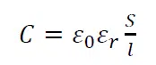
where
- ε0 = permittivity of vacuum
- ε r = relative permittivity of the dielectric material
- S = surface of electrodes
- l = thickness of dielectric
In order to achieve maximum capacitance value, εr relative permittivity of the dielectric material, surface area of electrodes shall be high, and the dielectric shall be as thin as possible. The capacitor must operate reliably at defined voltage in addition, so the dielectric shall feature high electric field strength in order to use a thin dielectric layer at desired working voltage. Surface area of electrodes is also important, and it may be related to the thickness of dielectric layer, as thin dielectric can follow fine structures / pores and thus create large surface area. This is especially important with increase of rated voltage of the capacitors as the thicker, high voltage dielectrics may not follow fine structure of electrodes. Thus, low voltage capacitors may successfully use nano/microstructure electrode materials, while high voltage capacitor electrodes has to be optimized for thicker dielectrics and also handling of much higher charging / discharging currents as the energy increase with voltage squared.
Selection of the right dielectric materials and capacitor construction is influenced also by other requirements such as required operation temperature range, high peak temperature withstanding during PCB mounting, humidity, vibration robustness, long lifetime etc.
3. HIGH ENERGY DIELECTRIC MATERIAL STUDY
3.1. High Energy Dielectric Materials – Overview
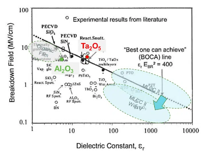
There were number of experiments and reported record high permittivity values achieved on various dielectrics since Figure 1. Chart was published by Pushkar in 2004. Nevertheless, the trials on such results achieved in laboratory conditions have not yet brought a breakthrough in practical “stable” and “useful” capacitor technology in mass production on the marker yet.
If we look what is a major change on capacitor technology market across past decades, one can notice a major increase of ceramic dielectric technologies that outperformed the other in number of sectors – miniaturization, cost, high voltage, stable parameters and reliability, low leakage current etc. Indeed, there are still some downsides on ceramic capacitor features and application limitations, nevertheless the fact that this technology has seen a major multi-level improvement across the past years and decades can be clearly noticed.
Aim of our research was thus focus to high energy and high voltage ceramic dielectric materials to check how / if we can achieve some improvements over the BOCA line and mass used dielectric types today.
If we look at Figure 1. chart from Pushkar at col. [1] and highlight domain of the currently most used technologies in mass production we can see that MLCC class II technology may outperform the others on first look into specifications, nevertheless the real application usage has to reflect its capacitance drop with applied voltage that may significantly degrade its energy storage capabilities, especially at high voltages. … Thus, it is also below BOCA line of max energy achieved. See Figure 1.
Note: the highest energy capacitor dielectric on the market is still tantalum wet electrolytic technology that reach energy density as high as 8J/cc at 250V, nevertheless high cost and higher ESR of this technology limit its use to a specific field such as medical implantable defibrillators.
Unlike tantalum capacitor technology, ceramic dielectric materials offer much higher potential of further development and flexibility to adjust its material characteristics and thus our focused was towards this direction of material research.
3.2. High Energy Ceramic Dielectric Materials
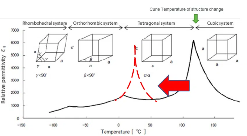
The highest energy density on ceramic dielectric materials is achieved with class II ceramic materials with ferroelectric features usually based on barium titanate BaTiO3, where the polarisation (capacitance) is created by its crystal structure.
BaTiO3 has a cubic crystal structure above the Curie temperature (approx. 125°C or more). It turns into a tetragonal crystal structure that creates a dipole, respectively domains of dipoles with different dipole orientation below the Curie temperature.
The dielectric material grain size/shape/distribution may impact number of dipoles and domains and thus its features and characteristics. The maximum permittivity and capacitance value is achieved at Curie temperature area around 125°C for a standard pure BaTiO3 material.
4. EXPERIMENTAL
4.1. Development Task
BaTiO3 ceramic dielectric material are the most common, proved dielectric material used in mass production of ceramic capacitors today. Due to its structure, the maximum capacitance value is achieved nearby Curie temperature ~ 125°C. There are number of applications with limited requirements on operating temperature range that may not require such wide temperature range – such as wearable electronics. Thus, can we modify BaTiO3 structure to achieve even higher energy density even at limited temperature range?
Modify BaTiO3 ceramic dielectric material by doping and optimization of its processing/structure to lower Curie temperature closer to room temperature and obtain suitable ceramic dielectric with high energy density. See Figure 2.
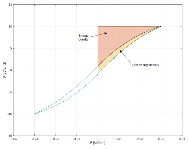
Combination of three key parameters of the dielectric will be monitored and targeted for best match: permittivity, electrical field strength and dielectric losses. The dielectrics will be benchmarked using P-E charts that is considered as best for energy storage capability assessment:
4.2. Selection of Suitable Ceramic Dielectrics Candidates
The approach to the development of high energy density take advantage of the unique properties of ceramic materials based on BaTiO3 (barium titanate – BT). These materials exhibit high dielectric as well as piezoelectric constants. Dielectric (and piezoelectric) properties are influenced by the technology of ceramic preparation process (e.g. particle size of starting ceramic powders, calcination and sintering temperature profile, ceramic density/porosity, or fired ceramic grains size), however crucial is also the impact of dopants added to the BaTiO3 ceramic (e.g. Ca, Sn, Nb, Co) and/or the composition of different barium and titanium based ceramic mixtures.
On the base of the literature search two ceramic materials were chosen for initial research:
- Lead-free ceramic 0.55(Ba0.9Ca0.1)TiO3-0.45Ba(Sn0.2Ti0.8)O3 (further denoted as BSCT), where excellent piezoelectric properties in the temperature range about 40°C were expected [4 to 7]. Due to that coincidence of piezoelectric and dielectric properties are observed in most cases, this ceramic was included.
- System BaTiO3-xBaSnO3 where the composition with x = 11 was chosen as the most promising one. (further denoted as BT-11BS) Here the relative permittivity maximum is observed for the Curie temperature close to 42°C. Reported dielectric constant peak value is about 70 000 at this temperature [8].
4.3. Sample Preparation Methods
Preparation of ceramic dielectric materials consist of two basic steps: (i) material synthesis and (ii) fabrication of the sample disc.
Features and electrical behaviour of ceramic materials are depending to number of structure parameters such as grain size, homogeneity, grain boundaries, material density, purity and other parameters.
Each synthesis and fabrication methods have its advantages and limitations. Selection of the method depends to requirements on dopant type, its quantity, duration of the test etc. and it may result in quite wide range of final parameters.
In our test preparation initial powder was mixed/milled, dried, sieved, calcinated, milled, dried, and sieved as the basic synthesis sequence resulting in a structure with mixed particle sizes. The synthesised material was then fabricated by three different processing methods referred further as: Process 1, Process 2. and Process 3.
5.TEST RESULTS
Test results are presented for ceramic disc samples made of three different ceramic dielectric materials:
- BT – pure BaTiO3
- BCST – 0.55(Ba0.9Ca0.1)TiO3-0.45Ba(Sn0.2Ti0.8)O3
- BT11BS – BaTiO3-11BaSnO3
5.1. BT – Pure BaTiO3 – Reference Ceramic Material Evaluation
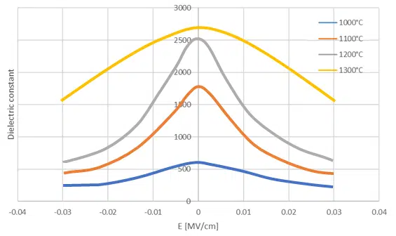
Figure 4. shows the dependence of dielectric constant on the electric field for different sintering temperature of BT prepared by Process 1. We can see that the dielectric constant value increases with sintering temperature, which is a result of higher density achieved within the sintering.
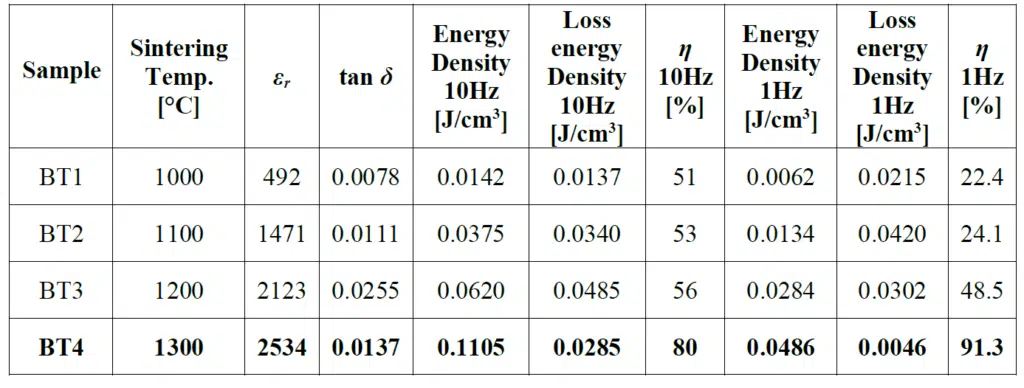
The summary of results measured on reference samples of barium titanate ceramics is given in Table 1.
Here the Energy storage density, Loss energy density, Efficiency of charge/discharge cycle determined from P-E loops measured at frequency 1 Hz and 10 Hz, and εr and tan δ measured at frequency 1 kHz is shown. Sintering temperature 1300C showed the best results with high efficiency above 90% @1Hz.
5.2. BCST 0.55(Ba0.9Ca0.1)TiO3-0.45Ba(Sn0.2Ti0.8)O3 Ceramic Material Evaluation
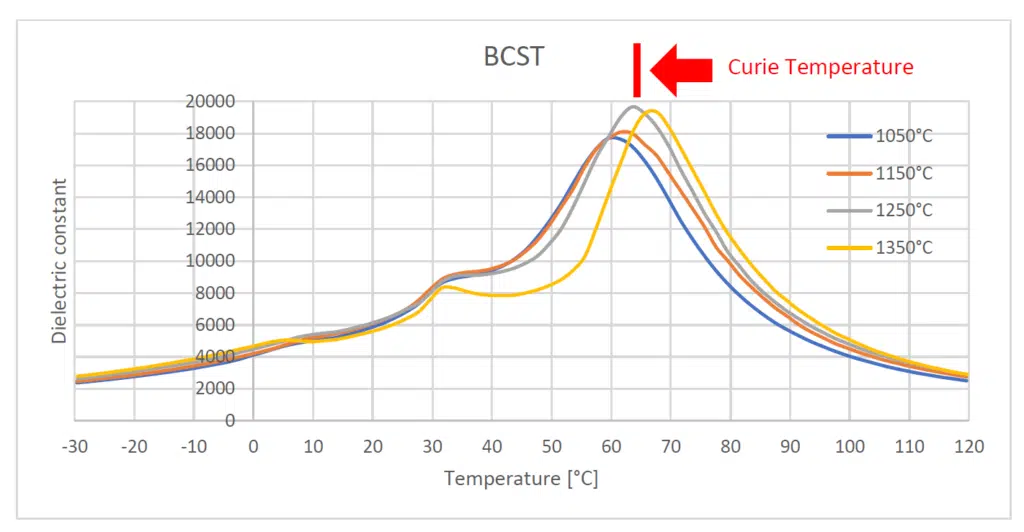
Due to S-shape of measured P-E loops characteristic the increase of BCST energy storage density with electric field is small. The efficiency of charge/discharge process is below 70 %. The dependences of dielectric constant on the temperature in the range -30 to 120°C is shown in Figure 5. for different calcination temperatures of BCST ceramic. We can see the shift of dielectric constant peak value on the Curie temperature with calcination temperature. The lower is the calcination temperature, the lower is Curie temperature. The Curie point is between 60 and 68°C in this case.
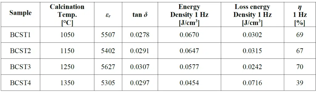
The summary of results measured on reference samples of BCST ceramics is given in Table 2. Here the Energy storage density, Loss energy density, Efficiency of charge/discharge cycle determined from P-E loops measured at frequency 1 Hz, and εr and tan δ measured at frequency 1 kHz is shown.
BCST results vs pure BT
The BCST dielectric key parameter differences versus pure BaTiO3:
- Curie temperature lowered from ~130°C to ~65°C
- Higher dielectric constant (2x in relative comparison to our reference samples)
- 40% increase of energy density vs reference BT sample
- Higher dielectric losses, efficiency below 70%
BCST evaluation summary
The BCST dielectric material shows increase of dielectric constant and energy density versus reference pure BT material, however the material shows high level of dielectric losses that disqualify this ceramic material as suitable capacitor dielectric.
5.3. BT-11BS BaTiO3-11BaSnO3 Ceramic Material Evaluation
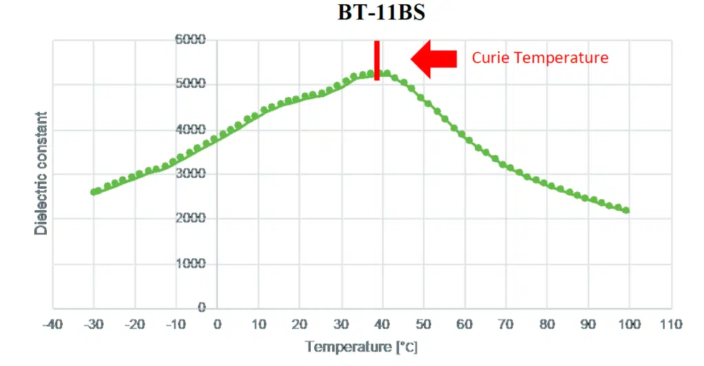
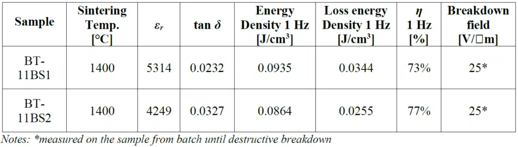
P-E loops measured at frequency 1 Hz for two BT-11BS samples prepared at calcination temperature 1150°C and sintering temperature 1400°C confirmed efficiency of charge/discharge process in the range 73 to 77%. Curie temperature of BT-11BS material, where the peak of dielectric constant value is obtained, is slightly above 37°C – see Figure 6., that may find a benefit for wearable applications operating at human body temperature.
The summary of results measured on reference samples of BT-11BS ceramic is given in Table 3. Here the Energy storage density, Loss energy density, Efficiency of charge/discharge cycle determined from P-E loops measured at frequency 1 Hz, and εr and tan δ measured at frequency 1 kHz is shown.
Energy density vs Electrical Field
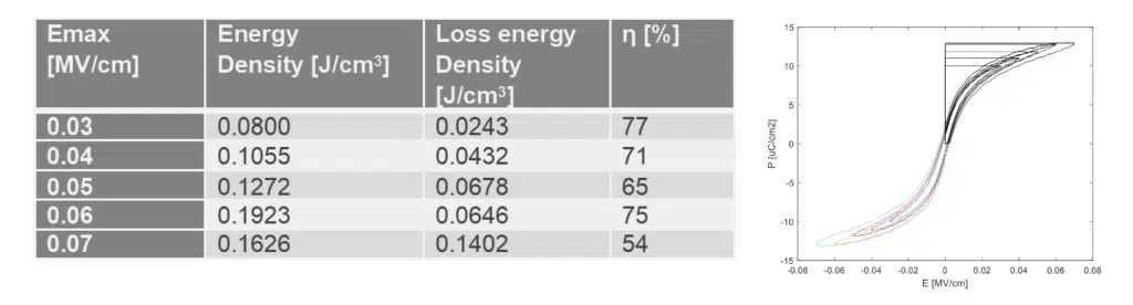
Samples of the BT-11BS were also subjected to evaluation of impact of high electrical field to obtained energy density values – see Tab 4 and illustration impact to P-E characteristics. The highest energy densities achieved was 0.19J/cc at 6V/mm electric field, and 75% efficiency.
BT-11BS results vs pure BT
The BT-11BS dielectric key parameter differences versus pure BaTiO3:
- Curie temperature lowered from ~130°C to ~37°C
- Higher dielectric constant (2x in relative comparison to our reference samples)
- High electrical field strength above 7kV/mm
- Up to 4x higher energy density vs reference BT sample
- High efficiency above 75%
BT-11BS evaluation summary
The BT-11BS dielectric material shows increase of dielectric constant and energy density versus reference pure BT material while efficiency is also kept at high level. The BT-11BS material shows high potential for further evaluation as a high energy, high electrical field capacitor dielectric material.
6. BT-11BS OPTIMISATION as CERAMIC DIELECTRIC MATERIAL
BaTiO3-xBaSnO3 ceramic system permittivity and its piezo characteristics have been already studied in scientific papers [8], however the main scope was to maximize its permittivity to achieve best piezo-electric features. Figure 7 is showing its crystal structure changes versus temperature and confirms that BT-11BS feature the highest permittivity among the BT-xBS system according to [8].
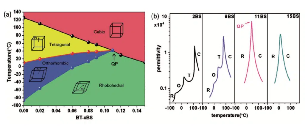
The BT-11BS material has a cubic crystal structure in temperatures above 37°C and rhobohedral structure in lower temperatures according to the source. It shall be noted that the peak high relative permittivity on BT-11BS in reference around 70K may achieve a good feature for piezo-electric applications, but it may not be optimized for capacitor dielectric where electrical field strength and dielectric losses may degrade its high energy storage capabilities.
The maximum of the BT-11BS dielectric constant was found to be ~ 17K at 41 °C on material prepared in reference [9]. The recovered energy density was 0.08 J/cm3 and 91% efficiency at 60 °C and the BT-11BS was considered as a potential material for further energy storage capability study.
Our next task for BT-11BS optimization as capacitor dielectric material included:
- preparation of the ceramic material by different techniques to achieve homogeneous microstructure with good functional properties.
- preparation of the ceramic material using different particle size to evaluate its impact to the material features.
- perform capacitance measurements and characterization
BT-11BS Particle Size Structure Optimization
For the optimization of this ceramic system, we studied the impact of particle size and sintering temperature for samples synthesized by Process 2. and Process 3. methods. Particle size of the ceramic powder was 100nm and 5μm, respectively. Four different sintering temperatures were chosen: 1380°C, 1400°C, 1420°C and 1440°C. This technology tuning resulted in eight different samples, which were further evaluated.
6.1. BT-11BS Optimization Results and Discussion
BT-11BS Process 2. Test Summary
BT-11BS material in its first evaluation showed some potential benefits with promising shape of E-P loop and efficiency above 75%. The impact of particle size and sintering temperature was studied on eight samples synthesized by the conventional solid-state method.
The optimized material prepared by conventional solid-state method showed increase of efficiency >80% and the permittivity up to 16K at 37°C temperature (~8K at room temperature) with overall energy densities around twice higher compared to pure BT reference sample (~0.1 J/cc @1Hz).
The increase of energy density as well as energy efficiency when operating the structure above the Curie temperature is an interesting finding illustrated in figures 30 and 31. The permittivity at temperatures above the Curie point is more stable with voltage.
The energy density may increase further with higher frequencies such as 100Hz and ED may increase in thin layers – for example prepared by tape casting MLCC manufacturing process.
BT-11BS Process 3. Test Summary
BT-11BS material prepared by Process 3. technique resulted in fine particle size, dense, homogenized structured material with different features compare to the materials prepared by Process 2. method.
The Process 3. material shows lower permittivity in range of ~ 3K at room temperature but increased electrical strength that allowed application of electrical field up to 0.09 MV/cm (vs 0.03 MV/cm in the case of conventional solid-state method).
Capacitance of Process 3. prepared samples drops at maximum voltage by ~50% vs ~80% drop on conventional methods (for comparable electric field). This results in significantly lower dependence of its permittivity / capacitance to applied voltage and increase of energy density at higher electrical fields.
The maximum energy density achieved was 0.4 J/cc at 82% efficiency, that is ~10x higher energy density compared to the reference pure BT material at 1Hz.
The Process 3. samples in our lab scale preparation had a limitation in too high thickness of test samples with very high breakdown voltage. Thus, to be able to analyse the sample disks in our test devices we had to grind and polish the sample to enable the measurement. These processes may degrade the pure material capabilities by some degree, thus in reality performance of the BT11-PS material prepared by Process 3. method may be even higher compare to the test results presented herein.
The energy density may increase further with higher frequencies such as 100Hz and it may present state of the art energy density in ceramic dielectric materials.
KEY FINDING: CAPACITANCE vs BIAS DROP IS MUCH LOWER ABOVE CURIE TEMPERATURE
The reason for the increase of energy density and Efficiency of charge/discharge cycle observed on BT-11BS materials can be determined from the dependence of the dielectric constant on the applied voltage (electric field on the sample). Figure 8 shows the dependence of dielectric constant on the applied voltage in the range -800 to +800 V for five different temperatures in the range approx. 25°C to 70°C.
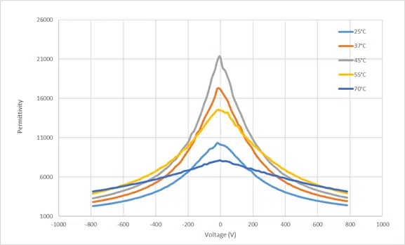
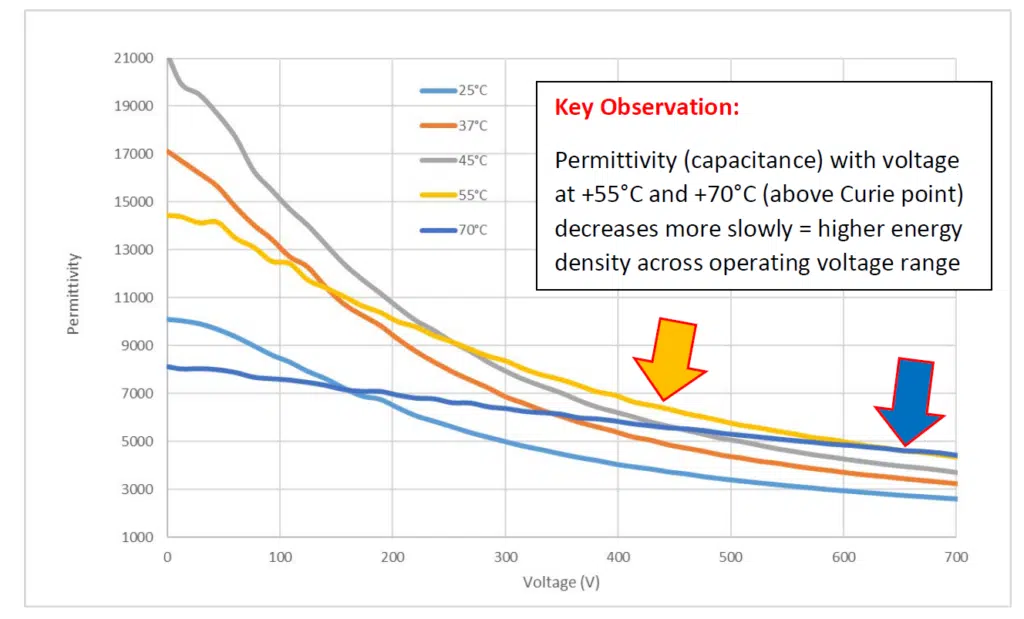
Dielectric constant decreases with increased electric field for all temperatures, but the closer we are to the Curie temperature (about 46 °C for these samples), the higher is both peak value of dielectric constant as well as the dielectric constant value for maximum applied voltage. However, for temperature above the Currie point the decrease of dielectric constant with electric field is considerably slower – see Figure 8. and Figure 9.
This phenomenon has been observed also in the case of pure BT reference material, and BCST material, where capacitance dependence with voltage was flatter for temperatures above the Curie Temperature. Based on this observation we can assume that this behaviour is not specific to the BT-11BS material, but common for ferroelectric ceramic dielectrics.
7. SUMMARY
- Methodology of using E-P hysteresis loop for dielectric material characterisation have been applied as the best suitable method for the first efficient evaluation at the existing lab scale environment.
- Ferroelectric BT-11BS known from its use in piezo devices was proved as the best candidate for high energy density ceramic dielectrics.
- BT-11BS material particle size and sintering temperatures have been subjected to optimization resulting in improvement of the material prepared by conventional solid-state synthesis method exceeding energy density of currently mass use pure BaTiO3 material.
- An interesting finding is that lowering Curie temperature of ferroelectric materials may increase electric density even further as the permittivity does not drop with voltage so rapidly when operating above the Curie temperature. This has been demonstrated on low Curie Temperature BT-11BS, BCST but also on pure BT material (at temperature of 160°C above CT). This behaviour is also not dependant to the fabrication process – observed in the same materials prepared by both Process 1., Process 2. and Process 3. methods, thus it can be considered as a general feature of ferroelectric materials.
- Advanced method of material preparation using Process 3. method yielded into a sample with fine, dense particle structure and further improved ED values in range of 10x versus reference pure BT samples. BT-11BS samples prepared by the Process 3. method were too thick that was difficult to analyse, and it had to be grinded that may impact on the final performance. Thus, further room present for the process optimisation to achieve even better results.
- Other preparation technologies such as Tape Casting or Cold Sintering may be more suitable to prepare thinner layer of the BT-11BS material to fully evaluate its potential for MLCC technology.
8. CONCLUSIONS
The research presented in this report identified BT-11BS ceramic ferroelectric material as a potential candidate for high energy density storage dielectric material with advantages of use especially as a high voltage, high energy capacitor with a stable capacitance vs BIAS and temperature performance.
Particle size, sintering temperature and use of different manufacturing methods to prepare BT-11BS layer were subjected to our lab optimization to maximize its energy density and capacitance stability. The maximum achieved energy density in our lab was ~ 4-10x higher energy density compared to the reference pure BT material depending to the manufacturing process.
The highest energy density on BT-11BS (10x higher ED than BT reference) was achieved using Process 3. method that produced very fine, dense ceramic dielectric structure with lower permittivity ~3K at room temperature but increased electrical strength that allowed application of very high electrical field up to 0.09 MV/cm (vs 0.03 MV/cm in the case of conventional solid-state method). Permittivity/capacitance drop with DC voltage has been also much lower (~ 30% at high electric field) compare to conventional methods (~ 90%). Permittivity/capacitance is also very stable with temperature – within 10% change between 25°C and 100°C. Process 3. method may be especially suitable for high voltage SLCC single layer ceramic capacitors to further increase its energy density at high operating voltages over kV range.
Interesting finding of the research is that permittivity/capacitance of general ferroelectric ceramic materials operated above Curie temperature decrease less with BIAS voltage and thus its overall energy density is higher as demonstrated on all tested materials pure BT, BCST and BT-11BS. This may be especially beneficial at high voltage field i.e., high energy density and high voltage capacitors.
These findings present a potential focus for development of the next generation capacitor ceramic materials with low Curie temperature featuring higher energy densities compare to the current state of the art.
BT-11BS is readily available material used and known for its piezoelectric features in piezo devices. It can be prepared and processed into a standard paste form used in mass ceramic capacitor manufacturing today such as screen printing and tape casting, thus it can be considered as compatible with the existing ceramic capacitor high manufacturing volume process and equipment.
The presented results of our research may pose a potential for further domination and growth of ceramic technology over the other capacitor technologies in wide range of higher energy density capacitor applications from ultraminiature smartphones through automotive to renewable energies and medical.
9. ACKNOWLEDGEMENT
Authors would like to express thanks to Bernd Pretzlaff, Janosch Lichtenberger, and Volker Lang for their support and advise for this scientific result.
10. REFERENCES
- I.Pushkar, et col. Thin-Film Capacitors for Packaged Electronics; Springer book 2004
- EPCI European Passive Component Institute ABC of CLR online handbook on passive components https://epci.eu/ceramic-capacitors-class2/
- Xihong Hao A review on the dielectric materials for high energy-storage application, JOURNAL OF ADVANCED DIELECTRICS Vol. 3, No. 1 (2013)
- W.Li, Z.J.Xu, R.Q. Chu, P. Fu, G. Z. Zang. Large piezoelectric coefficient in (Ba1-xCax)(Ti0.96Sn0.04)O3 lead-free ceramics. J. Am. Ceram. Soc. 94 (2011) 4131-4133.
- W. Li, Z. Xu, R. Chu, P. Fu, G. Zang. Enhanced ferroelectric properties in (Ba1-xCax)(Ti0.94Sn0.06)O3 lead-free ceramics. J. Eur. Ceram. Soc. 32 (2012) 517-520.
- L. Zhu, B. Zhang, X. Zhao, L. Zhao, P. Zhou, J. Li. Enhanced piezoelectric properties of (Ba1-xCax)(Ti0.92Sn0.08)O3 lead-free ceramics. J. Am. Ceram. Soc. 96 (2013) 241-245.
- L. Zhu, B. Zhang, X. Zhao, L. Zhao, F. Yao, X. Han, P. Zhou, J. Li. Phase transition and high piezoelectricity in (Ba,Ca)(Ti1-xSnx)O3 lead-free ceramics. Appl. Phys. Lett. 103 (2013) 072905.
- Y. Yao, C. Zhou, D. Lv, D. Wang, H. Wu, Y. Yang, X. Ren. Large piezoelectricity and dielectric permittivity in BaTiO3-xBaSnO3 system: The role of phase coexisting. EPL, 98 (2012) 27008.
- S.Merselmiza, et col. High energy storage efficiency and large electrocaloric effect in lead-free BaTi0.89Sn0.11O3 ceramic; Ceramics International, June 2020, DOI:10.1016/j.ceramint.2020.06.163


