


")


This article is an excerpt based on ESA SPCD 2022 paper entitled “New Generation of Wafer-Scale, Hermetically Sealed Chip Fuse for Space Applications” written by Bruno Zemp, SCHURTER AG, Lucern, Switzerland. The paper was presented during the 4th ESA SPCD conference at ESA ESTEC, The Netherlands 11-14th October 2022. Published under ESA SPCD organisation committee permission.
INTRODUCTION
This paper aims to introduce a novel hermetically sealed chip fuse technology. Retrospectively, the basic technology of the well-established space grade SMD 1206 chip fuse from SCHURTER, referred to as MGA-S [1], was developed more than two decades ago.
The exceptional performance of this fuse enabled the development of the ESA ESCC 4008 [2, 3] qualified version MGA-S and became one of the market’s most accepted SMD fuse for space applications. As emerging private space companies disrupt the traditional industry, new market needs raise. In addition, new competitors on different supply chain levels enter as well.
This technology requires, however, a wide range of sophisticated manufacturing steps relative to standard chip fuses such as SCHURTER’s USF 1206, which might represent a competitive drawback in terms of cost control. While the MGA-S covers a nominal current range starting at 140 mA up to 3.5 A, recent market requests address either lower currents below 140 mA or higher than 3.5 A at voltage levels up to 125 Vdc.
Narrowing regulatory restrictions by the European Union (EU) on using hazardous substances seriously endanger this products market lifetime–e.g. if the directive exception of Restriction of Hazardous Substances (RoHS) related to lead (Pb) high melting point (HMP) solders for fuses would be banned. To overcome these potential risks while still fulfilling customer needs, development activities have been initiated at SCHURTER. They resulted in a concept for a new generation of wafer-scalable, hermetically sealed chip fuse platform. The pertinent test results and challenges encountered during characterizing in the rated current range from 50 mA up to 250 mA are discussed in this paper.
TECHNICAL APPROACH
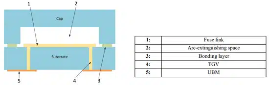
The approach orchestrates three key technologies: SCHURTER’s own state-of-the-art thin-film fuse link technology, a glass-wafer using through-glass via (TGV), and an advanced diffusion bonding technology to attain the hermetically sealed fuse body. The concept is a two-glass-wafer piggyback. The first substrate consists of the under bump metallization (UBM) representing the solder pads, then the metal-filled TGV for each pad which electrical links to the upper side, on the substrate’s top side there is the metal fuse link, and the outer bonding frame.
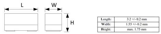
The upper substrate consists of the second metal frame and the cavity which might be filled with an arc-extinguishing substance of any condition, but here with a common silicone material that is utilized in many other fuses from SCHURTER. The simplified schematic in Figure 1 below demonstrates this concept on the chip level. The physical dimension on the chip level corresponds to the chip size SMD 1206.
TEST RESULTS AND FINDINGS
The discussion puts on the crucial tests which have been performed or are still ongoing at SCHURTER. These tests are namely the Breaking Capacity (BC), which is the capability of the fuse to interrupt safe at the maximal current and the rated voltage without getting mechanically damaged. Then a set of tests according to the ESCC 4008, explicitly the Thermal Vacuum (TV), the Operating Life, the Rapid Change of Temperature, and the Robustness of Termination are discussed. And finally, the hermetically sealing test results are introduced.
Electrical Figures
The concept targets a fast-acting type fuse, which means that it shall trip within 1 millisecond at 10 times the rated current (IR). The lowest overcurrent specified here is 2 times the IR and shall trip within 5 seconds. The maximal cold resistance of the smallest rated current design is 15 Ω, which is an acceptable value at this development stage. It is expected to reduce the ohmic value significantly by optimizing the TGV design and fuse link geometry, whereas the second mentioned is a trade-off between maximum BC and lowest ohmic losses.
| Rated Current | Max. Cold Resistance in Ω | Max. Voltage Drop in mV | Typ. melting I2t at 400 % of IR in A2s |
|---|---|---|---|
| 50 mA | 15 | 1200 | 0.00004 |
| 250 mA | 1.5 | 750 | 0.01 |
The typical cold resistance of the MGA 250 mA (MGA-S 175 mA) [1] is 0.8 Ω. This value is limited comparable to the corresponding samples discussed here. The current fuse link design is focused on maximizing the fuse’s melting energy I2t and BC capability. The I2t is approximately 10 times higher, also the BC performance is superior to the MGA-S.
The specific electrical resistance of the sample’s TGV material is approximately 2 times bigger than that of bulk copper. Consequently, the impact on the total resistance for bigger calibres having a low cold resistance of about 10 mΩ is tolerable small and the room for optimization of the cold resistance remains in the fuse link design (geometry and choice of metal).
Breaking Capacity
The BC is one of the fuse’s most decisive characteristics. In this study tests with 300 A (time constant of approx. 0.2 ms) at voltage levels starting at 63 Vdc to 200 Vdc have been performed.
| Design | Arc-Extinguishing Agent | 300 A at 63 Vdc | 300 A at 125 Vdc | 300 A at 150 Vdc | 300 A at 200 Vdc | Insulation Resistance at 500 Vdc |
|---|---|---|---|---|---|---|
| A | no | passed | failed | not tested | not tested | > 500 MΩ |
| B | yes | passed | passed | passed | passed | > 500 MΩ |
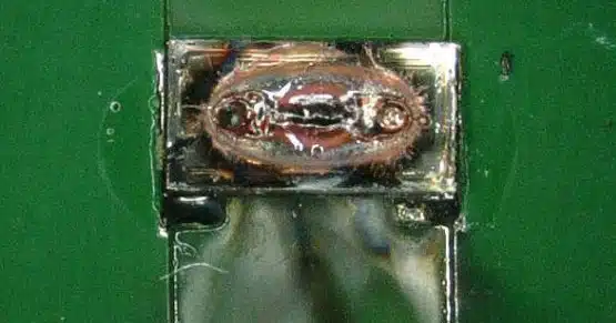
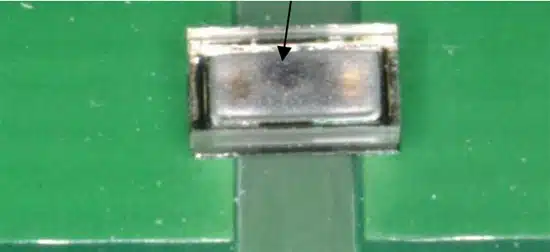
As to expect, the samples utilizing a silicone arc-extinguishing agent (design B) demonstrate significantly better BC performance than the ones without (design A). Design B passed any predefined test condition up to the maximal level of 300 A at 200 Vdc. In comparison to the datasheet of the MGA-S [1], the corresponding fuse calibre (MGA-S 262 mA) has a BC of 300 A at 125 Vdc.
Bad result!
Fuse body exploded, strong outgassing residuals.
Good result! Dark spot inside the body represents vaporized metal and arc-extinguishing agent material.
Thermal Vacuum test based on ESCC 4008 para. 8.15
Six samples of different rated current designs were considered in the Thermal Vacuum (TV) test. One sample showed a significant drift of +7.73 % after the test, while inside the acceptance limit of +/- 10 %. The root cause was narrowed down to the intermetallic joining between the UBM and the TGV. The visual inspection showed an indication of a starting crack in the glass surrounding the TGV. Similar observations were noticed in the Rapid Change of Temperature test.
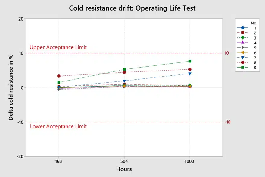
Operating Life Test based on ESCC 4008 para. 8.8
All samples were powered with 90 % of the calculated rated current. Three out of nine samples show significant, but quasi-linear elevating cold resistance drift over time. The root cause is not yet understood while the test is continuing until 50 % of them failed due to cold resistance’s acceptance limit violation or the minimal 2’000 hours is reached. Again, the acceptance limit of the relative cold resistance drift is +/- 10 % to the initial value.
Rapid Change of Temperature according to ESCC 4008 para. 8.9
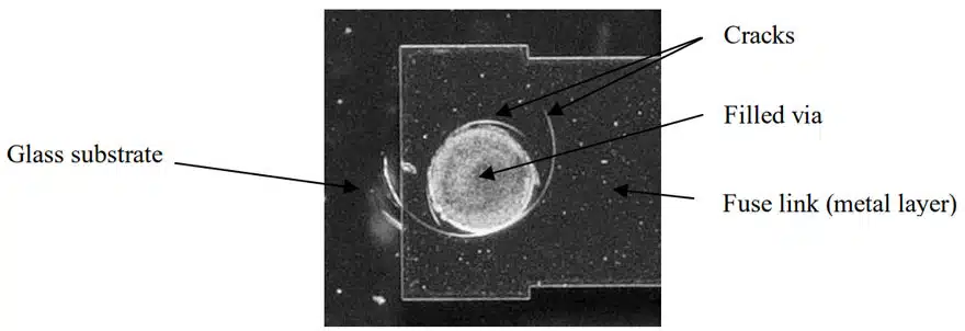
This test result was awaited with great interest as the thermal mismatch of the metal-filled vias and the glass substrate might cause serious inner-mechanical stress. Nine samples were tested. After the test four of them showed a significant cold resistance drift bigger than the acceptance limit of +/- 10 %.
Noticeable glass cracks surrounding the TGVs were observed in all failed samples. These cracks cause detachment and partial disconnections between the filled via and the fuse link (metal layer).
Robustness of Termination according to ESCC 4008 para. 8.14
This relatively simple test gives a good impression of the mechanical robustness of the UBMs. The test samples are soldered on a PCB test board according to the IEC 60127-4 [4] for miniature fuses. According to the ESCC 4008, the bending depth for surface mount fuses is 1 (- 0 + 0.5) mm. The cold resistance’s acceptance limit again is +/- 10 %.
Two samples were subsequently tested with a bending depth of 2.5 mm. The cold resistance of both changed by approximately + 50 % to the initial value. The root cause was narrowed down to the UBMs. Partial detached areas between the glass substrate/via and the metal pad were noticed.
Fine Helium Leak Test
A vital screening procedure before getting the samples subject to the electrical and mechanical tests discussed above is the hermeticity test. A fine helium leak test was performed with 36 samples. First, the samples were subjected to a pressurized He atmosphere to accelerate gas ingress into the fuse’s packaging.
The helium bombing in the chamber lasts for 72 hours at 5 bars. Then the samples were removed and leaking He was measured with a fine helium leak tester. The maximum acceptable leak rate is 1*10-9 mbar l/s. All samples passed, whereby four samples showed slightly higher values but were still 50 times below the maximum acceptable limit.
CONCLUSION
In this paper, test results of a novel hermetically sealed chip fuse technology utilizing SCHURTERs thin-film technology, wafer-scalable TGV substrates, and advanced packaging technology are discussed. The concept shows promising BC results, as the first samples passed the test conditions of 300 A at 200 Vdc. Therefore, in a consecutive test campaign, the BC performance shall be further investigated by increasing the supplied current and voltage until surpassing the chip fuse’s design limit.
The hermeticity of the packaging has been verified in a sophisticated fine helium leak test. The results from Thermal Vacuum and Operating Life confirm the expected respectable electrical long-term stability of the thin-film-based fuse link. The most critical part is the lacking performance of the TGV. Hence, the thermal expansion mismatch between the glass substrate and the filled vias must be further reduced. Further optimization comprises different ways of improving the mechanical stability of the glass layer. A trade-off must be found leading to an improved electrical conductivity while aligning the thermal expansion coefficient of the metal-filled-vias to the glass substrate.
In conclusion:
Preliminary results are utmost promising as the bottleneck related to TGV’s insufficient quality is likely to be resolved by the mentioned improvements.
REFERENCES
[1] Data Sheet MGA-S, September 2022, SCHURTER AG, www.schurter.com/en/datasheet/MGA-S
[2] ESCC Generic Specification No. 4008, FUSES, Issue 4, July 2015, ESCC Secretariat, Noordwijk, NL ESCC
[3] Detail Specification No. 4008/002, FUSES, 5 TO 15 AMPS BASED ON TYPE HCSF, Issue 1, September 2015, ESCC Secretariat, Noordwijk, NL
[4] International Standard IEC 60127-4, Miniature fuses – Part 4: Universal modular fuse-links (UMF) – Through-hole and surface mount types, Edition 3.2, December 2012, Geneva, C


