


")


Silicon MIS and MOS Capacitors
Silicon-based dielectrics are used within semiconductor manufacturing processes of high density electronic devices by semiconductor manufacturing processes. Silicon based dielectrics for capacitor technologies are usually based on silicon dioxide (MIS) or silicon nitride (MOS) insulating layers. Figure below describes a conventional MOS technology to make silicon capacitors.
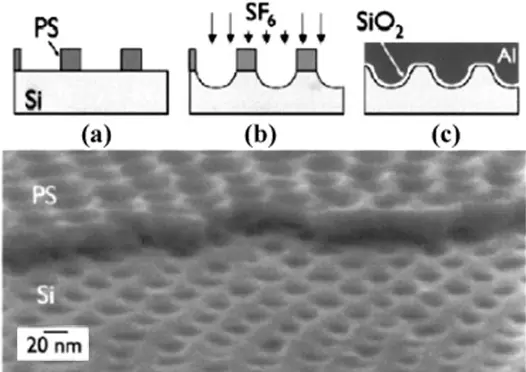
Conventional Technology MOS Capacitor Process
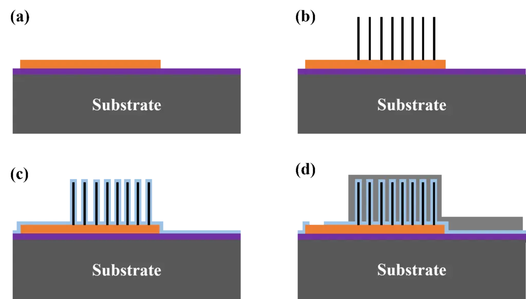
(a) Polymer template formation on silicon surface
(b) RIE pattern transfer of PS template into silicon, followed by the removal of the PS matrix.
(c) SiO2 growth followed by top Al gate electrode deposition
Silicon capacitors can be manufactured and used as
- fully MIS/MOS compatible back-end technology as part of passive integration platform
- hetero-integrated as Multiple-Chip-Module or flip-chip with other technologies (CMOS, MEMS, etc.) in a system in chip (SiP) or on chip (SoP)
- discrete chip SMD capacitors
Single Layer RF Silicon Capacitors
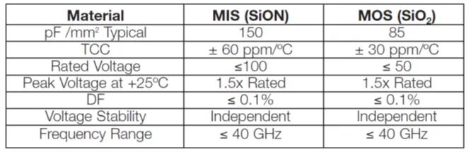
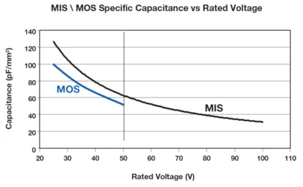
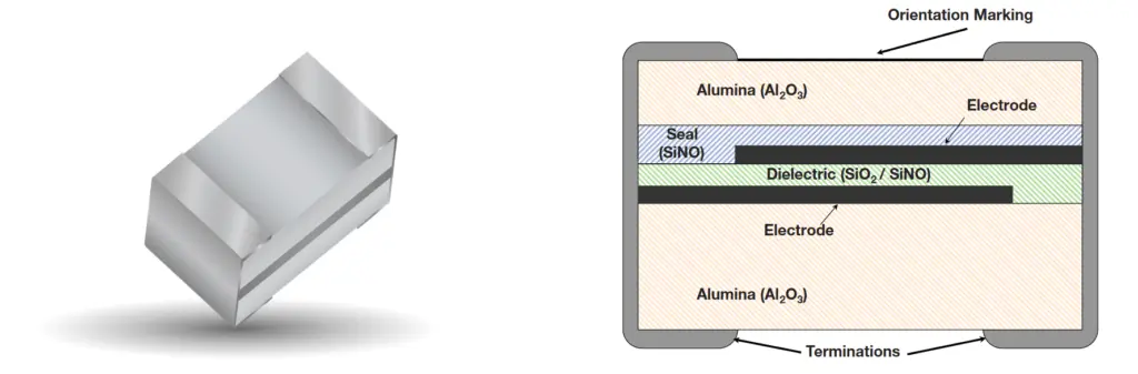
Silicon-based dielectrics are used to make low loss, high Q capacitors that feature very high temperature stability, high breakdown voltage and low leakage parameters. The main limitation is relatively low permittivity. Comparison of MIS and MOS dielectrics – see figure below.
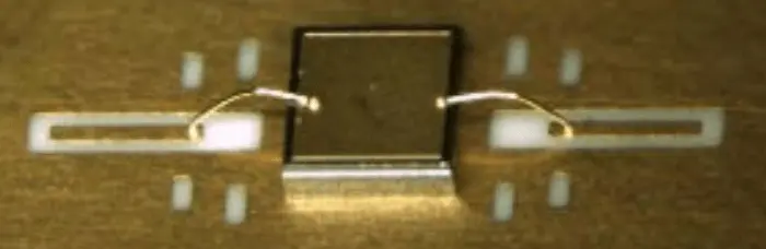
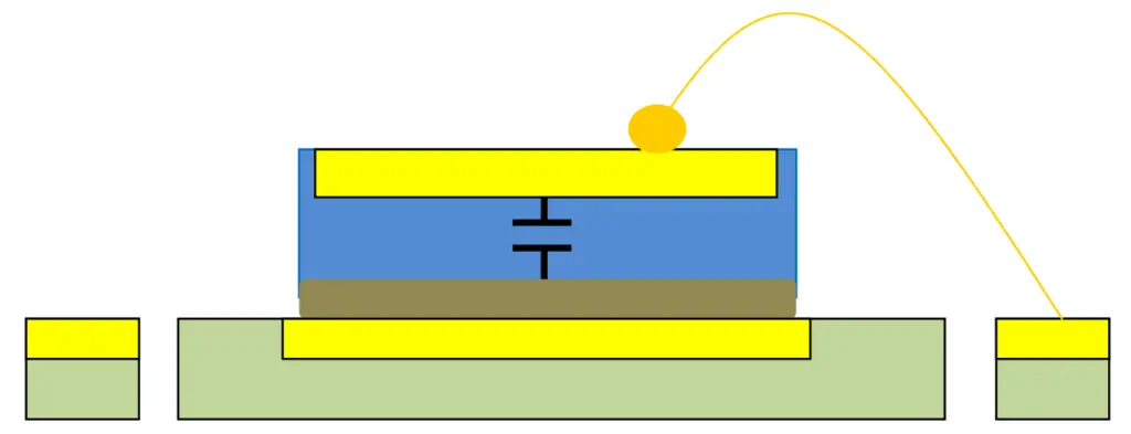
Gold or aluminum wire thermosonic and ultrasonic bonding are the most common way to assemble the single layer silicon capacitors (SLCs) in RF applications. Termination styles may differ and it can be optimized for epoxy or solder die attach mounting techniques.
RF Thin Film Silicon Capacitors
Silicon thin film capacitors are typically based on a single layer silicon oxide/nitride dielectric deposited on a substrate and packed in a chip MLCC like design. It offers unique ability of very low capacitance values (0.05pF) and very tight capacitance tolerances (±0.01pF). Thin film technology guarantees minimal batch to batch variability of parameters at high frequency and thus it is an ideal component for RF and microwave filters.
The term “thin film capacitors” however relates to a wider range of thin film technologies using also other dielectrics such as ceramic or organic films deposited on various substrates types such as alumina, quartz, silicon or silicon wafer.
Thus, distinction between “thin film”(deposited on silicon substrate) and “silicon” capacitors is something of a marketing concession, though significant differences exist within & among the two depending on the intended application.
Devices targeting RF tuning & matching applications tend to be low-capacitance, single-layer devices optimized for parameter stability and consistency, and are commonly found in standard JEDEC package sizes.
In contrast, devices intended for power supply decoupling, broadband DC blocking, and similar applications allow larger tolerances in favor of achieving higher specific capacitance, and are more likely to be found in packaging adapted to advanced assembly methods such as wire bonding or embedding within a PCB. Regardless of intended application however, devices in the thin film and silicon capacitor families are premium-performance products and are priced accordingly, currently fetching something on the order of 5 to 5000 times the price of ceramic devices with similar capacitance and voltage ratings.
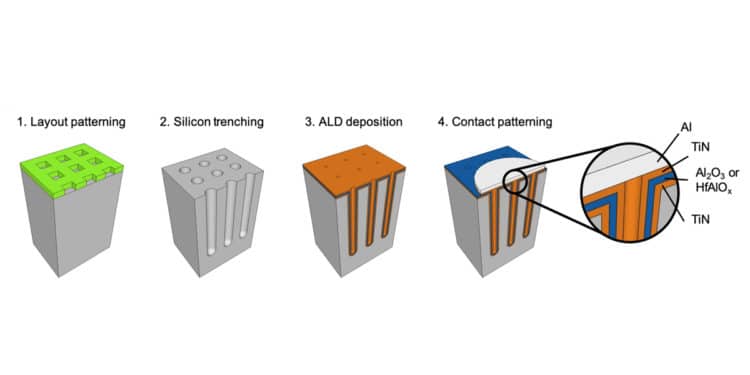
3D Silicon High Density Capacitors
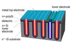
High density silicon capacitors are usually fabricated in ultra-deep trenches to increase surface area of electrodes. They have very low leakage current and low loss factor. Passive integration connective substrate (PICS) is the most common technology for implementing high density capacitors. This process allows implementation of multi-chip modules (MCMs) and chip on board (COB), and it helps to realize smaller components with low power consumption. In addition, this process allows integration of many basic functions into a single product, thereby helping to cut manufacturing costs. See figure below 3D PICS capacitor structure.
By employing latest 3D technologies, high volumetric efficiencies above 450nF/mm2 have been achieved. Silicon capacitors can be manufactured in layers below 100um that are 4xthinner than those of multilayer ceramic capacitor (MLCC) technology. Manufactured of silicon capacitors are claiming 10x better reliability in comparison to MLCC capacitors and in combination with ultra high temperature stability up to 250C, the high density silicon capacitor technology enable number of high demanding applications in automotive, industrial/oil drilling or aerospace/defense industry. It is expected that the volumetric efficiency of silicon capacitors will continue to improve as the demand for high performance and miniaturised components continues to grow.
Silicon capacitors – key features
- High Q, low losses
- Thin layers sub 100um possible
- High temperature operation (up to 250C)
- High reliability lifetime expectancy (10x better than MLCC, as example: full rated 10V continuous operation at 250°C for 50years)
- Low leakage < 30nA/mF; Higher leakage current at high temperatures (but still 1000x lower compare to the other technologies)
- No/low radiation sensitivity
- No derating required
- No catastrophic failure mode
- Low weight
- Stable performance with tight capacitance tolerances
- No piezo effect
- Non-magnetic
- Relatively low permittivity
Silicon Wafer Based Integrated Capacitors
Integrated capacitors and passives have a lot going for them. They take up less space on a PCB, they simplify design and they can, with the right processes shrink circuit tolerances thanks to closer component matching. The downside is that, as with semiconductors, volume is everything.
Although a common reason for keeping passive components off-chip is their size relative to that of the transistors on-die – is not worth wasting precious silicon area on devices that cost more to assemble than their materials are worth – many off-the-shelf parts rely on passives to tune filters and control loops for specific applications.
Utilization of semiconductor fabrication processes, however, has resulted in number of new approaches towards high density micro-capacitors. Finish company Picosun used its atomic layer deposition ALD equipment, to deposit film stacks of conductive TiN and insulating dielectric Al2O3 and HfAlO3 layers into high aspect ratio trenches etched into silicon that increased capacitance density up to 1 µF/mm2
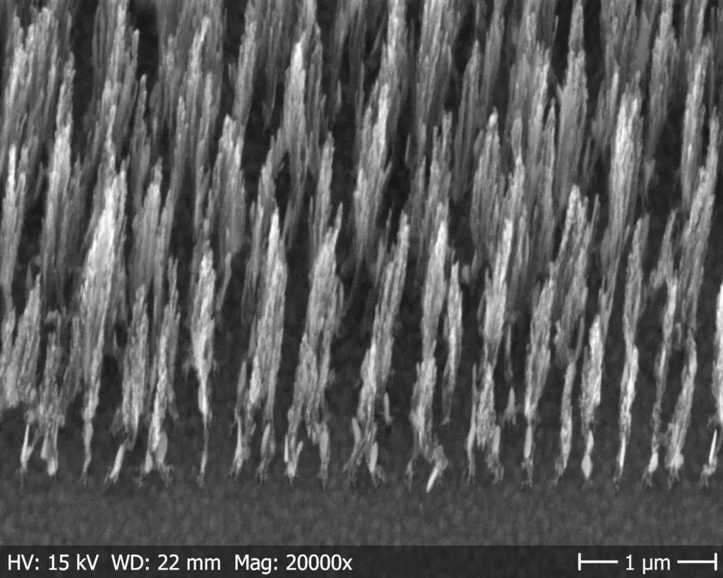
Swedish company Smoltek received Outstanding Paper Award at EPCI PCNS conference for their carbon nano-fiber metal-insulator-metal (CNF-MIM) wafer based semiconductor technology achieving capacitance density to +650nF/mm2 at the end of 2019. They used ALD technique to deposit Al2O3/HfO2 layers onto carbon nano-fiber 3D structure.
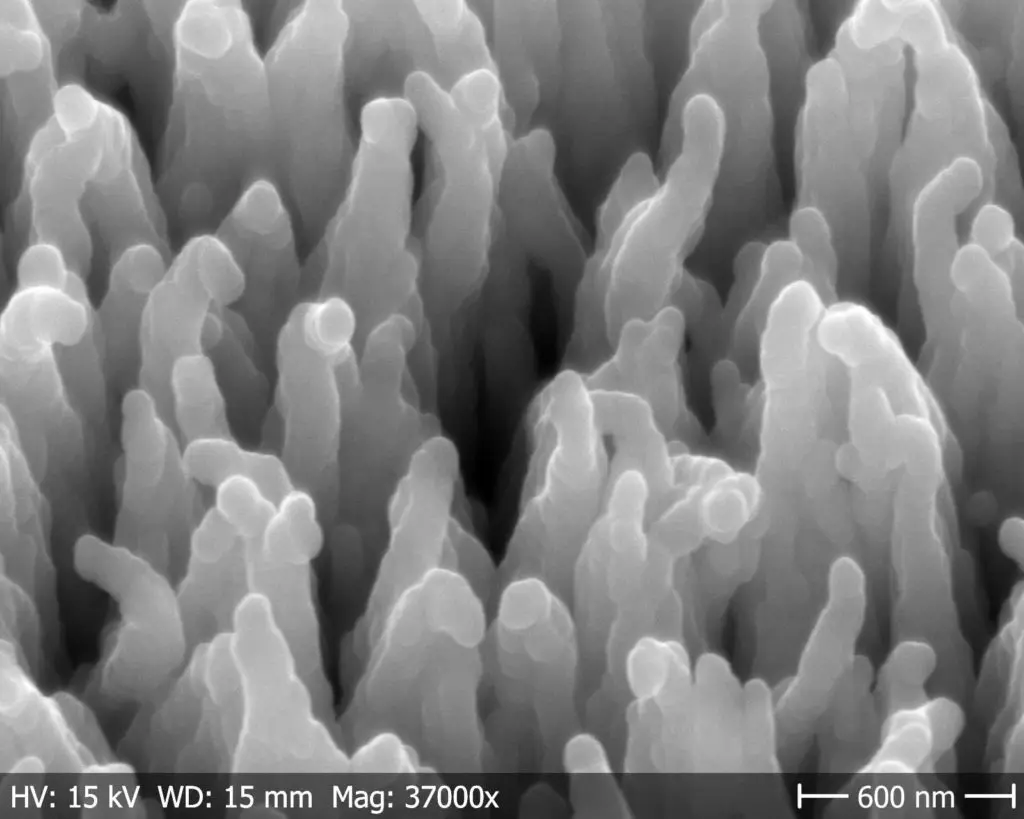
The fiber length is only 2 – 3 µm and the total height profile of the complete device is ca 4 µm. This makes the capacitors readily available for integration onto a CMOS chip or in 3D stacking. Figure below shows the CNFs after the dielectric coating via ALD, the image showing a coating of Al2O3/HfO2/Al2O3 (5/3/5 nm). The dielectric layer is uniformly covering the individual CNFs.
ABC of CLR: Chapter C Capacitors
Silicon and Silicon Wafer Based Integrated Capacitors
EPCI licenced content by:
[1] EPCI European Passive Components Institute experts original articles
[2] CLR Passive Components Handbook by P-O.Fagerholt*
*used under EPCI copyright from CTI Corporation, USA

This page content is licensed under a Creative Commons Attribution-Share Alike 4.0 International License.
see the previous page:
< Page 15a >
see the next page:


